Category Archives: PCB Layout
Common Circuit Design Reference & Precautions In PCB Design
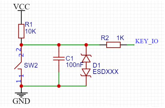
1. Common Design Reference of Keying Circuit 1)The R1 pull-up resistor clamps the [...]
Apr
Differential Lines Routing Requirements & Operation Skills In PCB Design
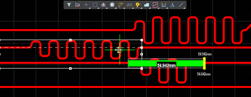
The popularity of high-speed serial buses has made more and more differential signals on the [...]
Apr

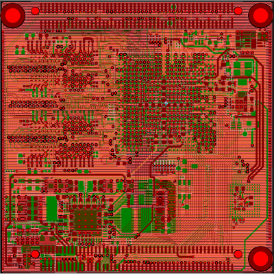
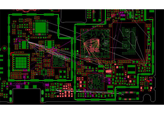
The Difference Between PCBSchematic & PCB Design File
Newbies often confuse “PCB schematic” and “PCB design file” when talking about printed circuit boards, [...]
Mar
Attention Points In High Frequency PCB Design
The rapid development of science and technology determines that all enterprises must improve accordingly. Among [...]
Mar
Precautions For Copper Clad In PCB Design
Copper clad is an important part in PCB design. Whether it is domestic PCB design [...]
Mar
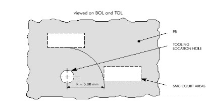
What Are The Requirements & Specifications of Fiducial Mark In PCB Design?
In order to facilitate the assembly of the printed circuit board (PCBA), fiducial mark will [...]
Mar
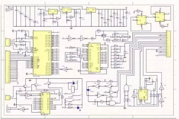
Schematic Reverse Method In PCB Reverse Engineering
Schematic Reverse in PCB reverse engineering is a common item. Grande, a professional PCB Reverse [...]
Mar
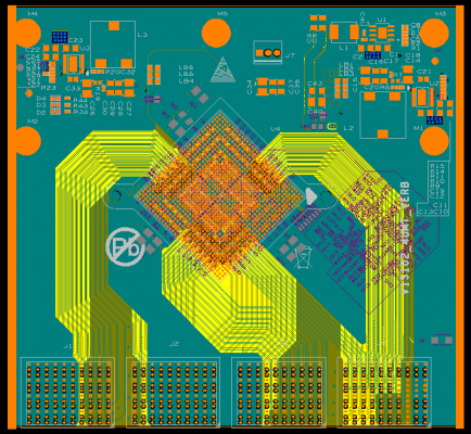
Which Aspects of The PCB Have An Impact On The PCBA?
As we all know, the PCBA manufacturing process is a quite complex process. The entire [...]
Feb
What Are The Size & Shape Requirements For PCB Design?
The simple truth of PCB design is that it must be suitable for its intended [...]
Feb
Are Gerber Files Important For PCB Assembly?
We need Gerber files and BOM list for PCB Assembly. It is helpful in PCB [...]
Dec