Category Archives: PCB Layout
What is The General Tolerance In Multilayer PCB Design?
How to Solve The Tolerance Problem in Multilayer PCB Design? No doubt, multilayer PCB is [...]
Dec
When Does PCB Design Safety Require Specific Spacing Rules?
As you probably know, not every PCB Design has the same strict rules like the [...]
Dec
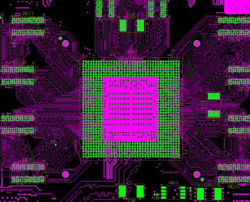
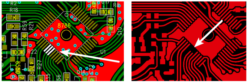
Design Standards of PCB Pads Shape & Size
Design standards of PCB Pads Shape & Size PCB Design is based on the circuit [...]
Nov
What is the PCB design window? What is the use of opening windows in PCB design?
What Is Solder Mask Opening? Generally, the leads on the PCB are covered with solder [...]
Oct
PCB Design Standards of Pads Shape & Size
PCB Design is based on the circuit schematic diagram to realize the functions required by [...]
Oct
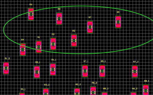
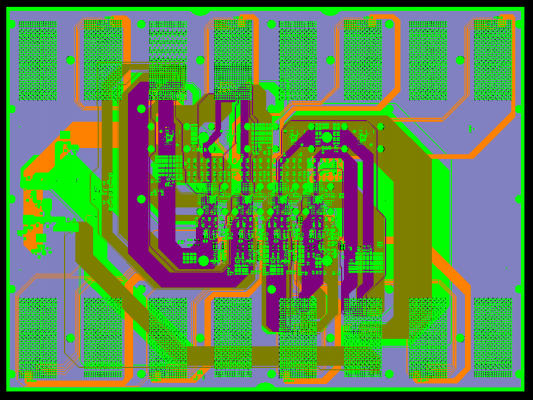
Components Arrangement Discipline In PCB Design
In current PCB design, there are 5 regular disciplines, components arrangement discipline, according to the [...]
Oct
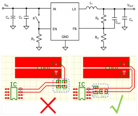
Main Points In PCB Layout
In integrated circuit application design, after the project schematic design is completed, PCB design is [...]
Sep
Eight Things Need to Consider Before PCBA Mass Production
1) Consider the design scale before choosing components Which is more important for board size? [...]
Aug
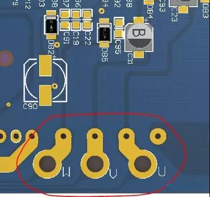
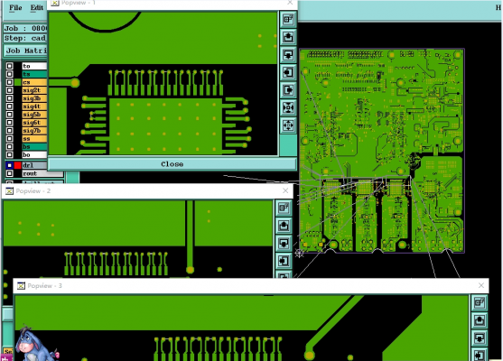
Why do Pads lost and Pads deformation occur in PADS ( PCB Design Software) ?
At present, most high-speed PCBs are designed via Cadence, PADS software and Altium Designer (AD). However, Companies [...]
Jul

Types of Pads In PCB Layout
What Is Pad? Pad, the basic unit of surface mount assembly, which is used to [...]
Jul