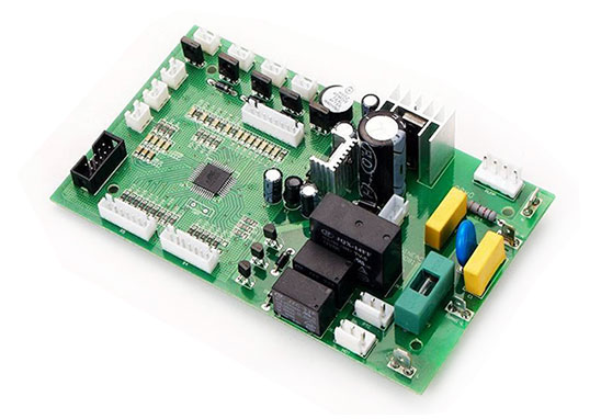
PCB Design is based on the circuit schematic diagram to realize the functions required by the circuit designer. PCB design mainly refers to the layout design, which needs to consider various factors such as the layout of external connections, the optimized layout of internal electronic components, the optimized layout of metal connections and through holes, electromagnetic protection, and heat dissipation. Excellent PCB design is ablt to save production costs and achieve good circuit performance and heat dissipation performance.
Common Pads Shapes In PCB Design
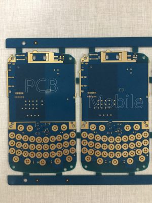
Pads can be divided into 7 categories, which are distinguished by shape as follows:
1. Square pad-It is often used when the components on the PCB are large and few, and the printed wires are simple.
2. Circular pads-widely used in single and double-sided boards with regularly arranged components.
3. Island-shaped land-the connection between the land and the land is integrated, and is often used in vertical irregular arrangement.
4. Teardrop pad-It is often used when the connecting trace is thin, and is often used in high-frequency circuits.
5. Polygonal pads-used to distinguish pads with close outer diameters but different apertures for easy processing and assembly.
6. Oval pad-This kind of pad has enough area to enhance the anti-stripping ability, and is often used for dual in-line devices.
7. Open-shaped pad-In order to ensure that after wave soldering, it is commonly used when the manually repaired pad hole is not sealed by solder.
PCB Design Standards of Pads Shape & Size
1. The minimum single side of all pads is not less than 0.25mm, and the maximum diameter of the entire pad is not more than 3 times the component aperture.
2. Try to ensure that the distance between the edges of the two pads is greater than 0.4mm.
3. In the case of dense wiring, it is recommended to use oval and oblong pads.
4. For plug-in components, in order to avoid copper foil breaking during soldering, the single-sided connecting plate should be completely covered with copper foil, and the minimum requirement for double-sided panels should be filled with teardrops.
5. All machine insert parts need to be designed as drip pads along the bent leg direction to ensure full solder joints at the bent leg.
6. The pads on the large-area copper skin should be chrysanthemum-shaped pads, not to be soldered.
The above is an introduction to the design standards for the shape and size of the pads in PCB design. If you have PCB design and PCBA requirements, welcome to contact us. Next, we will introduce our PCB design capabilities and PCBA processing capabilities.
PCB Design Ability
The highest signal design rate: 10Gbps CML differential signal;
The highest number of PCB design layers: 40 layers;
Minimum trace width: 2.4mil;
Minimum trace spacing: 2.4mil;
Minimum BGA PIN spacing: 0.4mm;
Minimum mechanical hole diameter: 6mil;
Minimum laser drilling diameter: 4mil;
Maximum PIN number:; 63000+
Maximum number of components: 3600;
Maximum number of BGA: 48+.
PCBA Capability
1. The largest board: 310mm*410mm (SMT);
2. Maximum board thickness: 3mm;
3. Minimum board thickness: 0.5mm;
4. The smallest component: 0201 package or parts above 0.6mm*0.3mm;
5. The maximum weight of mounted parts: 150 grams;
6. Maximum component height: 25mm;
7. Maximum component size: 150mm*150mm;
8. Minimum lead component spacing: 0.3mm;
9. The smallest spherical component (BGA) spacing: 0.3mm;
10. The smallest spherical component (BGA) diameter: 0.3mm;
11. Maximum component placement accuracy (100QFP): 25um@IPC;
12. Mounting capacity: 3 to 4 million points/day.