Category Archives: PCB Blog
Blog
What Is The Meaning Of “Plugged Vias” In PCB Manufacturing Process?
There are three common methods to deal with via holes in PCB boards:Tenting vias,Plugged vias [...]
Jan
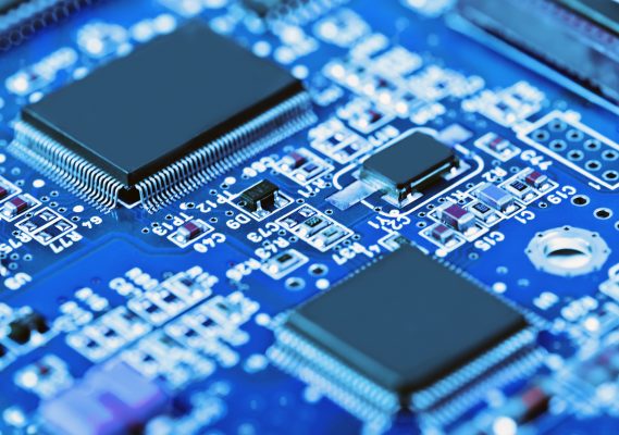
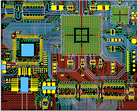
PCB Board Heating Serious Reason
In integrated circuits, excessive temperature can negatively affect the function, components and the board itself. [...]
Dec
SMT Processing Requirements For PCB Design Component Layout
SMT processing for PCB design component layout is a requirement. Reasonable layout planning in the [...]
Nov

PCB Design Lecture: The Meaning And Function Of PCB Layers
PCB is a multi-layer structure, different layers have different purposes.Let’s Grande to introduce the meaning [...]
Nov
Solutions For White Circles When PCB Design Wires And Pads
Will you encounter this situation when doing PCB design? The trace and the pad with [...]
Nov
The Method For PCB Design That Can Withstand 100A Current
The usual PCB design current will not exceed 10A, or even 5A. Especially in household [...]
Nov
Mark Point Design Specification In PCB Design
Mark points, also called datum points, provide a common position-able circuit pattern for all steps [...]
Nov
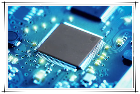
What Is The Mean Of Opening In PCB Design?
Before introducing the PCB design opening, we first need to know what the solder mask [...]
Nov
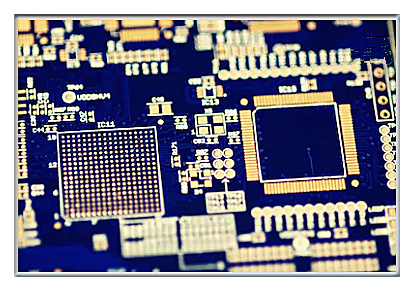
What Are The Production Difficulties Of Multi-Layer PCB Proofing, Do You Know?
Multi-layer PCB board in communications, medical, industrial control, security, automotive, electric power, aviation, military, computer [...]
Nov
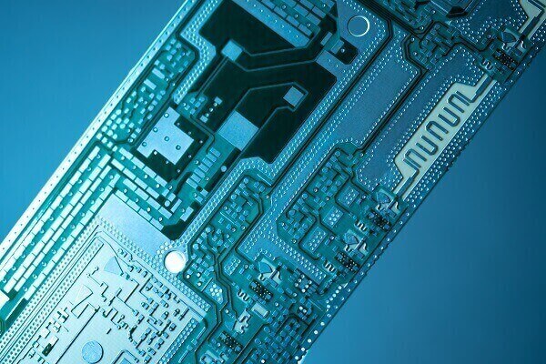
Six-Layer PCB Design Laminated Solution For EMC Compliance
PCB board lamination structure is an important factor affecting its EMC performance and an important [...]
Oct