Will you encounter this situation when doing PCB design? The trace and the pad with a white circle, it seems as if nothing is wrong with the wiring. But just do not know where the wrong. Some people had to delete the trace and redraw it to eliminate the error, or simply ignore the error. So how to solve this problem?
The wrong solution.
Method 1: Press the “T + M” key, it disappears, visually comfortable. Does not affect the effect of PCB proofing back.
Method 2: Click “DXP” -> “Parameter Selection” -> “PCB Editor”, the “Online DRC ” in front of the hook to remove. Better than the first method. In fact, these two methods are to ignore the error, which is not correct.
The correct solution.
First we run the design rule check inside the toolbar, you can see an error report, according to the error prompt, in go to the toolbar to find the design rule. Then follow the diagram below.
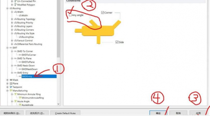
In fact, it is the angle of the connection between the trace and the pad, check any angle (any angle), you can fundamentally solve this error. Because the root of any error can be found in the rules. Encounter the error is to solve the error, not to ignore it!
Grande is a PCB design company specializing in electronic product circuit board design (layout wiring design). It mainly undertakes multi-layer, high-density PCB design drawing boards and circuit board design proofing business. The PCB design team with an average of more than 10 years of work experience can proficiently use the mainstream PCB design software in the market, professional and efficient communication to ensure the progress of the PCB design, and help you seize the market opportunities earlier!