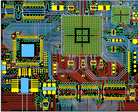
PCB board lamination structure is an important factor affecting its EMC performance and an important means to suppress electromagnetic interference. Before the design of multilayer PCB board, it is necessary to determine the circuit size, board size and electromagnetic compatibility (EMC) requirements of the board structure used. Grande will introduce the six-layer PCB design laminated program in line with EMC design.
Six-layer PCB design laminated solution for EMC compliance
In some six-layer PCB design laminated solution,the shielding of electromagnetic fields is not good enough, and the reduction of transient signals in the power supply bus is minimal. That chip density, higher clock frequency design can be considered six-layer PCB design.
The first laminated solution: SIG-GND-SIG-PWR-GND-SIG.
This laminated solution can get better signal integrity, the signal layer is adjacent to the ground layer, the power layer and the ground layer are paired, the impedance of each alignment layer can be better controlled, and both ground layers can absorb magnetic lines well. In addition, with the power and ground layers intact, a good return path can be provided for each signal layer.
The second laminated solution: GND – SIG – GND – PWR – SIG – GND.
This laminated solution is only suitable for cases where the component density is not very high. This laminated has all the advantages of the above laminated , and the ground plane of the top and bottom layers is more complete this way, and can be used as a better shield layer. It should be noted that the power supply layer to be close to the non-main component side of the layer, because the bottom layer of the plane will be more complete. Therefore, EMI performance is better than the first solution.
For six-layer PCB design solution, in order to obtain better power and ground coupling, you should try to reduce the spacing between the power layer and the ground layer. Like the 62 mil board thickness of this, although the reduced layer spacing, it is not easy to control the spacing between the main power and ground layer is very small. The second option compared to the first option, greatly increased the cost, so we will generally choose the first option when set the laminated layers. In the design, to follow the 20H rule and mirror layer rule design.
Grande is a PCB design company specializing in electronic product circuit board design (layout wiring design). It mainly undertakes multi-layer, high-density PCB design drawing boards and circuit board design proofing business. The PCB design team with an average of more than 10 years of work experience can proficiently use the mainstream PCB design software in the market, professional and efficient communication to ensure the progress of the PCB design, and help you seize the market opportunities earlier!