Category Archives: PCB Layout

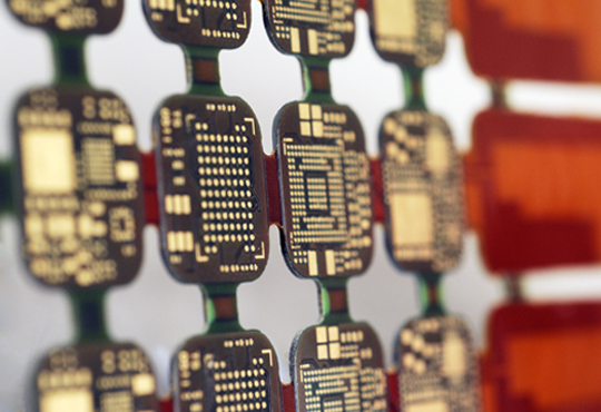
PCB Design Lecture: The Meaning And Function Of PCB Layers
PCB is a multi-layer structure, different layers have different purposes.Let’s Grande to introduce the meaning [...]
Nov
Solutions For White Circles When PCB Design Wires And Pads
Will you encounter this situation when doing PCB design? The trace and the pad with [...]
Nov

The Method For PCB Design That Can Withstand 100A Current
The usual PCB design current will not exceed 10A, or even 5A. Especially in household [...]
Nov

Mark Point Design Specification In PCB Design
Mark points, also called datum points, provide a common position-able circuit pattern for all steps [...]
Nov
What Is The Mean Of Opening In PCB Design?
Before introducing the PCB design opening, we first need to know what the solder mask [...]
Nov
Six-Layer PCB Design Laminated Solution For EMC Compliance
PCB board lamination structure is an important factor affecting its EMC performance and an important [...]
Oct

Solutions To Impedance Discontinuity Problems In PCB Design
We all know that the impedance need be continuous in PCB design. But there are [...]
Oct
Will The Wrong Design Of Silkscreen Bit Number Affect The PCBA Patch Processing?
When we do PCB design, pay great attention to the direction of the bit number [...]
Oct
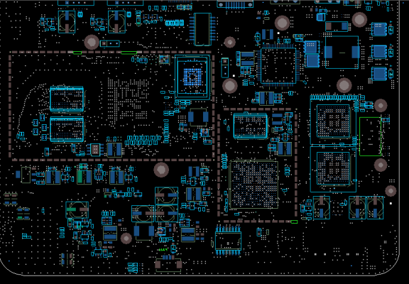
Detailed Description Of The Basic Flow Of PCB Design
PCB design is a very detailed work, so you should be very careful and patient [...]
Oct
Eight Common Technical Problems of PCB Design
PCB design technology is kind of complex and involves many problems in lots aspects. To [...]
Jul