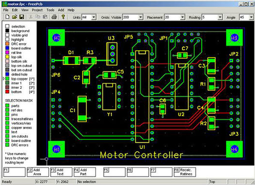
PCB is a multi-layer structure, different layers have different purposes.Let’s Grande to introduce the meaning and function of PCB layers.

The Meaning And Function Of PCB Layers
1、TOP LAYER (top wiring layer).
Designed for top layer copper foil wiring. The single layer is not need this layer.
2、BOTTOM LAYER (bottom wiring layer).
Designed for bottom copper foil alignment.
3、TOP/BOTTOM SOLDER (top/bottom solder mask green oil layer).
TOP/BOTTOM SOLDER GREEN OIL is laid to prevent tin on copper foil and maintain insulation. Solder mask green oil openings at the pads, vias and non-electrical alignments on this layer.
Solder pad will be opening by default in the design (OVERRIDE: 0.1016 mm), that is, the pad exposed copper foil, flared 0.1016 mm, wave soldering on the tin. It is recommended that no design changes be made to ensure solder ability.
The over-hole will be opening by default in the design (OVERRIDE: 0.1016mm), the over-hole will be exposed to copper foil and will be expanded by 0.1016 mm, which will be tinned during wave soldering. If the design to prevent tin on the hole, do not show copper, you must be additional properties of the hole SOLDER MASK (solder mask opening) in the PENTING option check, then close the hole opening.
In addition this layer can also be alone for non-electrical alignment, then the solder mask green oil corresponding opening. If it is above the copper foil alignment, it is used to enhance the over-current capability of the alignment, soldering with tin processing; if it is above the non-copper foil alignment, it is generally designed to do identification and special character screen printing, which can be omitted to make the character screen printing layer.
4, TOP/BOTTOM PASTE (top / bottom solder paste layer).
The layer is generally used for SMD components of the SMT reflow process when on the solder paste, and PCB manufacturers board has no relationship, export GERBER can be deleted, PCB design to keep the default.
5、TOP/BOTTOM OVERLAY (top/bottom silkscreen layer).
Designed for various silkscreen logos, such as component bit numbers, characters, trademarks, etc.
6, MECHANICAL LAYERS (mechanical layer).
Designed for PCB mechanical shape, the default LAYER 1 for the shape layer. Other LAYER 2/3/4, etc. can be used as mechanical size markers or special purposes, such as some boards need to make conductive carbon oil can use LAYER 2/3/4, etc., but must be clearly identified in the same layer the use of the layer.
7, KEEPOUT LAYER (prohibited wiring layer).
Designed to prohibit wiring layer, many designers also use to do PCB mechanical shape, if the PCB has both KEEPOUT and MECHANICAL LAYER 1, it mainly depends on the completeness of the shape of these two layers, generally MECHANICAL LAYER 1 prevail. It is recommended that the design try to use MECHANICAL LAYER1 as the shape layer, if you use KEEPOUT LAYER as the shape, then do not use MECHANICAL LAYER 1 again to avoid confusion !
8、MIDLAYERS (intermediate signal layer).
Mostly used for multi-layer boards, can also be used as a special purpose layer, but must be clearly identified in the same layer the use of the layer.
9、INTERNAL PLANES (internal electric layer).
Used for multi-layer boards.
10、MULTI LAYER (through-hole layer).
Through-hole pad layer.
11, DRILL GUIDE (drill positioning layer).
Solder pad and through-hole drilling of the center positioning coordinates layer.
12. DRILL DRAWING (Drill hole description layer).
Drill hole size description layer for pad and over hole.
