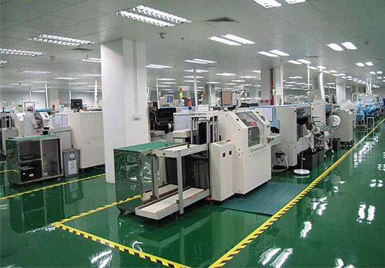
SMT processing for PCB design component layout is a requirement. Reasonable layout planning in the process of processing and production will play a role in helping. Layout issues if you do not consider the actual processing situation will cause some problems in production. And the layout requirements for different processing methods are different.
SMT chip processing component layout requirements
1, Replaceable, adjustable components:If need to often replace or adjust the components, parts, need to consider the characteristics of the whole machine and requirements, will be placed in the easy to replace the location.
2, Temperature-sensitive components: In the placement process, if encounter temperature-sensitive components, must be far away from heat-generating components, like triodes, integrated circuits, electrolytic capacitors, etc., are far away from high-power components, heat sinks and high-power resistors.
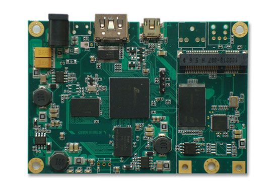
3, Alignment direction, in the SMT placement of the actual processing, SMD components alignment direction is also required, try to keep the same direction, the characteristics of the direction to be consistent, so as to facilitate the subsequent placement, welding and detection, especially the number of components printing direction must be the same.
4, Balanced distribution, higher quality SMD components in the process of re-flow soldering processing heat capacity will be greater than the general components, which will lead to local temperature differences and even virtual soldering problems, to maintain a balanced distribution in SMT processing can avoid such problems, but also to maintain the balance of the circuit board.
5, Heat-generating components, different components in contact with each other, will have an impact on other components, such as heat-generating components, such are generally placed in the corners, ventilation position, conducive to heat dissipation. Heat-generating components must be supported by other leads or supports, but also and the surface of the printed circuit board to maintain a certain distance, the minimum can not be less than 2mm, otherwise it will affect the quality of the board.