Category Archives: PCB Layout
The Role Of Matching Resistors In PCB Design
1.PCB design impedance matching PCB design impedance matching refers to a suitable matching method between [...]
Jul

Demystifying The Design Technics of High-End PCB
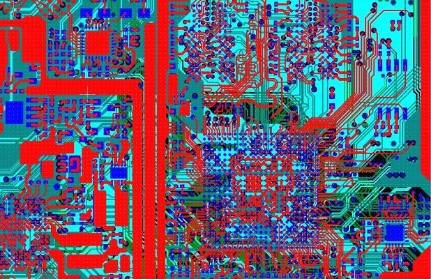
Plenty of people probably do not know the difference between high-end PCB and common PCB? Because there is not [...]
Jul
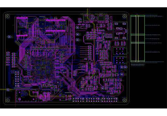
Why Most of PCB Layers Are Designed As Even Layer?
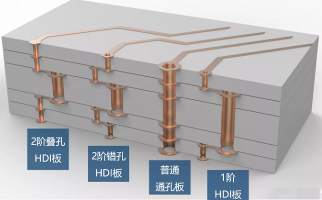
I don’t know if you have found such a phenomenon, that is, most of PCB layers are designed as even layers, such [...]
Jul
Why Need Add Fiducial Point & Technological Edge In PCB Design?
Reasons / Adding Fiducial Point When it comes to SMT Assembly, there are usually 3 common methods (based [...]
Jul
Q & A of PCB Layout Knowledge
Q1. What problems should pay attention to when layout high-frequency signals? A1. Impedance matching of the signal [...]
Jul

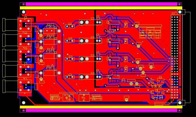
The Importance Of PCB Laminate Technology For PCB Layout
A good PCB laminate design is essential to reduce the radiation of PCB loops and related circuits. On the [...]
Jul
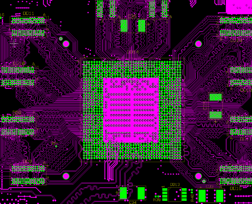
What Is The General Tolerance For Multi-Layer PCB Layout?
Multi layer PCBs are beneficial to products because they can handle greater complexity. Computers, telephones, and [...]
Jul
PCB Design & Layout Skills
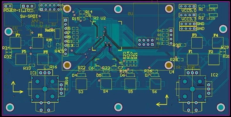
The following items need to be considered when conveying the Schematic to PCB layout. All the examples mentioned [...]
Jul

The Role Of Matching Resistors In PCB Design
1)PCB design impedance matching PCB design impedance matching refers to a suitable matching method between [...]
Jul
Demystifying The Design Technics of High-End PCB
Plenty of people probably do not know the difference between high-end PCB and common PCB? Because there is not [...]
Jul