Reasons / Adding Fiducial Point
When it comes to SMT Assembly, there are usually 3 common methods (based on the situation of using stencil ): Manual, semi-automatic and fully automatic soldering. So what’s the difference among them? Manual SMT, that is to brush the stencil and soldering electronic components by hand; Semi-automatic SMT refers to brushing the stencil manually but soldering electronic components via automatic SMT Machine; While Fully automatic SMT means that both brushing stencil and soldering electronic components are all fully automated by SMT Machines.
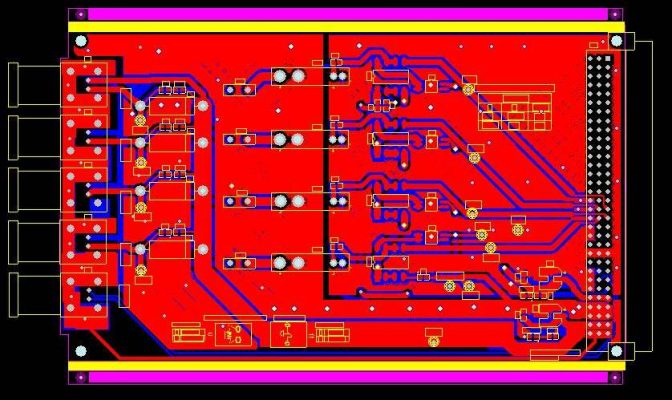
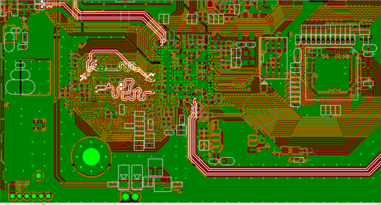
Manual soldering is easy for us to understand, after all, human beings are flexible and smart, and they can find ways to deal with emergencies during soldering. However, SMT Machine and relevant equipments are quite different, which definitely don’t know where to put electronic components on the right positions of PCB, such as exactly corresponding pads, correct the chip placing orientation, etc. In the “PADS Output BOM and Part Number Map”, which explains how to output the component coordinates, including the position and orientation information of every single component on the PCB, as shown in the following figure:
The Automatic SMT Machine exactly performs positioning in the light of the above mentioned datas. This is why fiducial point added in PCB Design. Because SMT Machine is going to identify this fiducial point as an positioning point, and then identify the position and orientation of electronic components based on the coordinate and orientation information. Furthermore, fiducial point is designed and placed on the diagonal of each board, and they appear in pairs. In addition, the rectangle drawn on the diagonal line should preferably include all the electronic components on the single board. By the way, fiducial point is also able to be made on the technological edge as long as which places on the diagonal line and appears in pairs.
Reasons / Adding Technological Edge
So why need add technological edge? Similarly, if PCB is manual soldering, the technological edgemay not necessary. Mainly considering, in PCB design, which will require more plates if adding technological edge. However, in order to be able to use the SMT Machine, it is necessary to add a technological edge while PCB design so that the SMT Machine can use the fixture to clamp the PCB. Sure, if a single PCB is relatively large and there are no electronic components 5mm from the edge of the board, the technological edge is not necessary, and the board can be directly clamped by the fixture. In addition to adding fiducial points on the technological side. Besides, positioning holes also need to be added and which is mainly used for testing.
Method Of Adding Technological Edge & Fiducial Point
1.Technological Edge
The width technological edge is not less than 5mm, and the length is as long as the board. Speaking of the application of technological edge, it can be used in both array and single boards. Meanwhile, technological edge is able to be marked with fiducial points and positioning holes. The positioning hole is a through hole with a diameter of about 3mm.
The manufacturing method of technological edge is actully much similar with board array, that is, using 2D lines to layout the same length as PCB and 5mm width on all layers, and then connecting with original PCB. The connection method can be V-cut, stamp hole or connecting strip according to actual needs. As for the specific operation process, you may google the video.
2.FiducialPoint
The fiducial point includes two parts: One is the mark in the middle with diameter of 1mm; The other is a circular open area around the dot, and the center of the circle coincides with the center of the mark in the middle whose diameter is 3mm.
Here is the detailed PCB Design method about fiducial point :
1)Enter the package editor and placinga circular patch pad with a diameter of 1mm on the top layer;
2)Placea copper foil hollow area with a diameter of 3mm on the top layer;
3)Placea copper foil with a diameter of 3mm on the top solder mask;
4)Finish and save it.
While using, enter the ECO mode directly and just add fiducial points to encapsulate. Pay attention to, there can be no traces and 2D lines in the open area around fiducial points. Finally, design PCB with technological edges, fiducial points and positioning holes.
Well, the above is the function and production method about technological edges and fiducial points. The specific details should be modified according to the requirements of the PCB manufacturer.