Category Archives: PCB Layout
Charging Rules & Requirements For PCB Prototype
Many novices are always confused about the charging rules and requirements for PCB Prototype and [...]
Jul
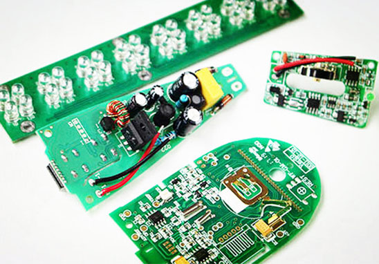
How To Prevent Others From Copying Board In PCB Design?
In PCB design, after completing the circuit board design through many levels, the most important [...]
Jul
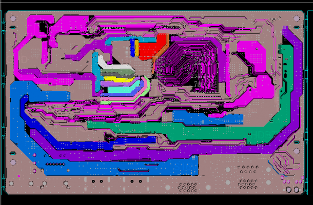
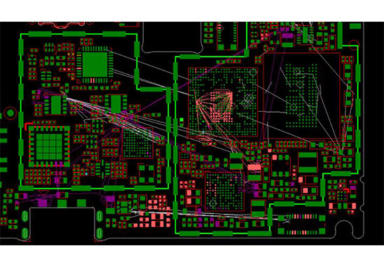
PCB Design Routing Measures To Reduce High-Frequency Signals Crosstalk
PCB design high-frequency circuit routing should pay attention to the “crosstalk” of near-parallel signal lines [...]
Jun
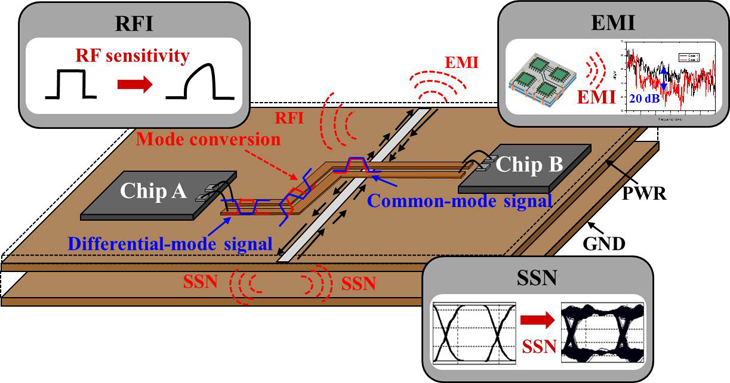
What Factors Are Related To EMC Issue In PCB Design?
The EMC issue in PCB design is vital and plays a decisive & surprisingly big [...]
Jun
Failure Checking Method On Newly Designed PCB Board
For a newly designed PCB board, it is often difficult to debug, especially when the [...]
Jun
How To Reduce The Impact of PCB Stray Capacitance?
When referring to electronic circuits on the PCBA, a term often used is stray capacitance. [...]
Jun
Common Problems in PCB Design
Grande is a PCB design company specializing in electronic product Circuit Board Design (PCB Layout). [...]
May
PCB Design Tips for Replacing ICs
In PCB design, when you need to replace the IC, then let’s talk about the [...]
May
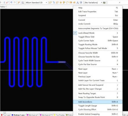
18 Special Trace Routing Methods & Techniques In PCB Design (1)
Special Trace 1– Altium Designer Routs Serpentine Trace Method If you choose Interactive length tuning [...]
Apr
Shielding Methods In High Speed PCB Design
The transmission rate of high-speed PCB design and routing system is accelerating with the changes [...]
Apr