The EMC issue in PCB design is vital and plays a decisive & surprisingly big role in the quality and performance stability of the PCB circuit board. So what factors are related to EMC issue in PCB design?
Factors Related To EMC Issues In PCB Design
1. System Design
When designing for system-level EMC, the first step is to identify the source of EMI interference, so that the source of EMI radiation can be gradually better shielded.
2. Structural Influence
If the radiation disturbance emission of non-metal chassis exceeds the standard, measures such as conductive spraying, local shielding design, cable shielding treatment, and reasonable grounding treatment should be taken.
3. Cable Influence
Do not use cable shields as signal return paths.
4. Component Selection
Take the varistor as an example: The main feature of the varistor is a wide operating voltage range, which plays the role of voltage protection, lightning protection, suppression of surge current, absorption of spike pulses, amplitude limiting, and noise reduction.
5. SI/PI Simulation
Before and after the EMC design of a single board is completed, it is necessary to carry out the overall EMC simulation comparison and verification of the single board, and even the improvement effects of some main EMC design measures need to be simulated and compared.
6. Ground
Grounding purpose: To establish a low-impedance path between the equipment casing and the nearby metal conductors. When there is leakage current in the equipment, it will not endanger personal safety.
7. The relationship of PCB design
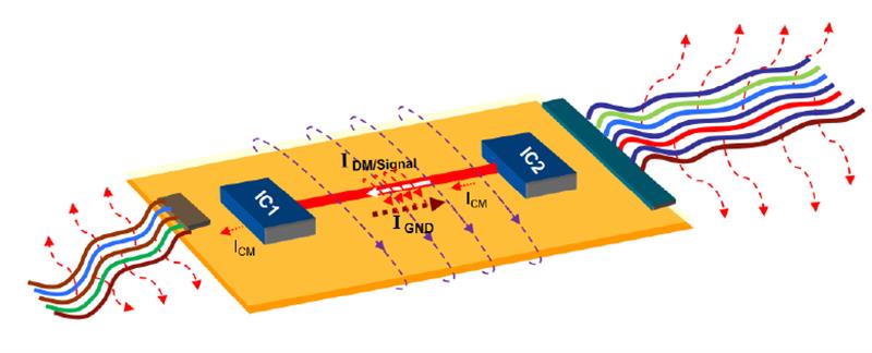
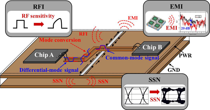
When the RF current in the PCB board passes, when the current passes through the closed circuit, a magnetic field is generated; at the same time, a radiated electric field is also generated. This is the main reason for the radiation interference caused by the switching power supply PCB board.
8. Software anti-interference technology
Including redundancy technology, fault tolerance technology, marking technology, digital filtering technology, etc.
9. Shield
An effective way to suppress interference in the form of a field is electromagnetic shielding.
10. Filtering
Filtering technology is the main means to suppress the conducted electromagnetic interference of electrical and electronic equipment and improve the level of conducted anti-interference of electrical and electronic equipment, which is also an important auxiliary measure to ensure the overall or partial shielding efficiency of the equipment.
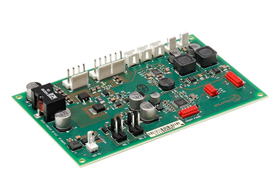
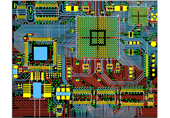
Grande PCB Design Capability
The Highest Signal Layout Rate: 10Gbps CML differential signal;
Maximum PCB Layout Layers: 40 layers;
Minimum Trace Width: 2.4mil;
Minimum Trace Spacing: 2.4mil;
Minimum BGA PIN Spacing: 0.4mm;
Minimum Mechanical Hole Diameter: 6mil;
Minimum Laser Drilling Diameter: 4mil;
Maximum Number of PINs: ;63000+
Maximum Number of Components: 3600;
Maximum Number of BGAs: 48+.