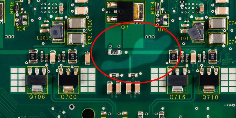
Blistering on the board surface is one of the common quality defects in the PCB production process. Due to the complexity of the PCB production process, it is difficult to prevent board surface foaming defects. So, what are the reasons for the blistering on the PCB surface?
Reasons For Blistering On The PCB Surface
1. The problem of substrate processing. For some thinner substrates, due to the poor rigidity of the substrate, it is not suitable to use a brushing machine to brush the board. Therefore, attention should be paid to control in the production and processing process to avoid blistering on the board surface due to poor adhesion between the base copper foil and chemical copper.
2. Oil pollution caused by board surface processing (drilling, lamination, milling, etc.), or dust pollution caused by other liquids, will cause the board surface to foam.
3. The copper brush board is bad. The pressure of the grinding plate before the copper sinking is too high, which leads to the deformation of the orifice, and the orifice foams during the copper sinking, electroplating, tin spraying, and soldering process.
4. Wash with water. Because copper plating requires a lot of chemical solution treatment, and there are plenty of kinds of acid, alkali, inorganic, organic and other medical solvents, it will not only cause cross-contamination, but also cause poor local treatment of the board surface, resulting in some adhesion problems.
5. Micro-etching in copper plating pretreatment and pattern plating pretreatment. Excessive micro-etching can lead to substrate leakage at the orifice and blistering around the orifice.
6. The activity of the copper precipitate is too strong. The content of the three components in the newly opened copper sinking bath or bath is high, which leads to the deterioration of the physical properties and quality of the coating, and the defect of poor adhesion.
7. Oxidation of the board surface during the production process will also cause the board surface to blister.
8. Poor rework of copper mines. During the rework process of some copper-plated rework boards, due to poor stripping, incorrect rework methods or improper control of micro-etching time during the rework process, there will be blistering on the board surface.
9. Insufficient water washing after development, too long storage time after development, or too much dust in the workshop during transfer of graphics and text, which will cause potential quality problems.
10. The pickling tank should be replaced in time before copper plating, otherwise it will not only cause problems with the cleanliness of the board surface, but also cause defects such as roughness of the board surface.
11. Organic pollution, especially oil pollution, will make the board surface in the electroplating tank blister.
12. In the production process, special attention should be paid to the charged feeding of the plate, especially the plating solution with air stirring.
The above is the analysis of the causes of blistering on the surface of the PCB. Hope it will be helpful to colleagues in the industry! In the actual production process, Sure thing, there are also many other reasons for the blistering of the board surface. It need to be analyzed on a case-by-case basis, not generalized.
Grande PCB Manufacturing Ability
Mass Production 2 to 14 layers, 14-22 layers can be produced by sample.
Minimum Trace Width/Spacing: 3mil/3mil BGA spacing: 0.20MM
Minimum Aperture of Finished Product: 0.1mm Size: 610mmX1200mm
Ink: Japan Tamura, Taiyo, Futoken;
FR4: Shengyi, Kingboard, Haigang, Hongren, Guoji, Hazens, South Asia,
(Shengyi S1130/S1141/S1170), Tg130℃/ Tg170℃ Tg180℃ and other high TG plates)
High Frequency Board: Rogers (Rogers), Taconic, ARLLON;
Surface Technology: Spray tin, lead-free spray tin, immersion gold, full board gold plating, plug gold plating, full board thick gold, chemical immersion tin (silver), anti-oxidation (OSP) blue glue, carbon oil