For a newly designed PCB board, it is often difficult to debug, especially when the board is large and there are many components, it is often difficult to get started; if you master a set of reasonable failure checking methods, debugging will be more effective. So, what are the failure checking method on newly designed PCB?
Failure Checking Method On Newly Designed PCB Board
1. Measuring Voltage Method
First, confirm whether the power supply pin voltage of each chip is normal, and then check whether various reference voltages are normal, including whether the working voltage of each point is normal.
2. Signal Input Method
Add the signal source to the input terminal, and then measure the waveform of each point in turn to see if it is normal, so as to find the failure point. Sometimes simpler methods can be used, such as touching the input terminals at all levels with tweezers to see if the output terminals respond, and which is often used in amplifying circuits such as audio and video; However, it should be noted that this method cannot be used for circuits with hot backplanes or high voltages, otherwise electric shock may occur. If there is no response at the upper level, but there is a response at the lower level, it means that the problem is at the upper level, and focus on checking.
3. See,Hear, Smell, Touch
“Look” refers to whether the component has obvious mechanical damage, such as cracking, blackening, deformation, etc.
“Listening” refers to hearing whether the sound at work is normal, such as something that shouldn’t be ringing, where it should be, or that the sound is abnormal.
“Smell” means to check whether there is any odor, such as burnt smell, capacitor electrolyte smell, etc.
“Touch” means to test whether the temperature of the component is normal; Some power components will heat up and work, if they feel cold, it can be judged that they are not working; If the place that should not be hot is hot or the place that should be hot is too hot, there is also a problem. In addition, you should be careful when touching, try to touch first, do not burn your hands.
Grande PCB Assembly Advantages
1)Strength Guarantee
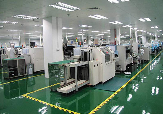
 SMT factory: With imported SMT machines and multiple optical inspection equipment, which is able to produce 4 million points per day. Each process is equipped with QC personnel who will keep an eye on product quality.
DIP production line: Two wave soldering machines and more than 10 employees who have worked for over three years. That’ s to say, these workers are highly skilled and can weld various SMT & DIP components.
2)Quality Assurance With High Cost Performance
High-end equipment can paste precision special-shaped parts, BGA, QFN, 0201 package. It can also be soldered prototype pcba via SMT machine and placing bulk materials by hand.
Both samples, small and large batches can be produced. And there is no SMT Machine starting cost.
3)Rich Electronic Products SMT Soldering Experience With Stable Delivery
Accumulated services to thousands of electronics companies, involving SMT soldering services for various types of automotive equipment and industrial control motherboards. Furthermore,PCBA Products are often exported to Europe and the United States, and the quality is able to be affirmed by new and regular customers.
4)Strong Maintenance Ability & Reliable After-Sales Service
The maintenance engineers have sophisticated experience so that those defective boards caused by all kinds of smt soldering can be repaired. Meanwhile, ensuring the connectivity rate of each circuit board also make sense.
Order problems feedback will get response, solution and solved as soon as possible.