PCB design high-frequency circuit routing should pay attention to the “crosstalk” of near-parallel signal lines introduced by signal lines. Crosstalk refers to the coupling phenomenon that there is no direct connection between signal lines. The parameters of the PCB layer, the distance between the signal lines, the electrical characteristics of the driving end and the receiving end, and the termination method of the signal lines have a certain influence on the crosstalk.
PCB Design Routing Measures to Reduce High-Frequency Signal Crosstalk
1. Insert a ground wire or a ground plane between two lines with severe crosstalk, which can isolate and reduce crosstalk;
2. If parallel distribution cannot be avoided, a large area of ”ground” can be arranged on the opposite side of the parallel signal lines to greatly reduce interference;
3. On the premise of allowing routing space, the distance between adjacent signal lines can be increased and the parallel length of the signal lines can be reduced;
4. If parallel traces in the same layer are unavoidable, then in two adjacent layers, the direction of the traces is vertical;
5. The clock line is surrounded by ground lines, and more ground holes are made to reduce capacitance distribution and reduce crosstalk;
6. For high-frequency signal clocks, try to use low-dropout minute signals and wrap them;
7. Do not suspend unused inputs, but ground or connect them to power.

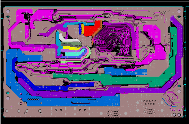
Grande PCB Design Capability
The Highest Signal Design Speed: 10Gbps CML differential signal;
Maximum PCB Design Layers: 40 layers;
Minimum Line Width: 2.4mil;
Minimum Line Spacing: 2.4mil;
Minimum BGA PIN Spacing: 0.4mm;
Minimum Mechanical Hole Diameter: 6mil;
Minimum Laser Drilling Diameter: 4mil;
Maximum Number of PINs: ;63000+
Maximum Number of Components: 3600;
Maximum Number of BGAs: 48+.
PCB Design Service Process
1. Customers provide schematic to consult PCB design;
2. Grande evaluates the quotation in the light of the schematic and customer design requirements;
3. The customer confirms the quotation, signs the contract, and prepays the project deposit;
4. Grande receives advance payment and arranges PCB Layout engineer to design;
5. After the PCB Layout is completed, Grande provides a screenshot of the document to the customer for confirmation;
6. The customer confirms OK, settles the balance, and provides PCB design information.