Special Trace 1– Altium Designer Routs Serpentine Trace Method
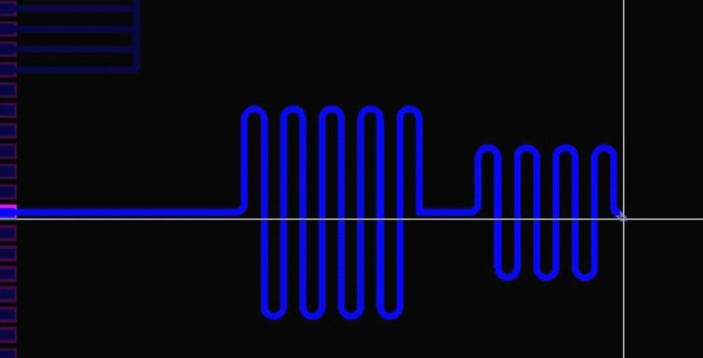
If you choose Interactive length tuning in the Tool, you need to rout the trace first and then change it into a serpentine shape. Here, the serpentine shape is used directly when routing: P->T routing first, and then Shift+A to switch to the serpentine shape.
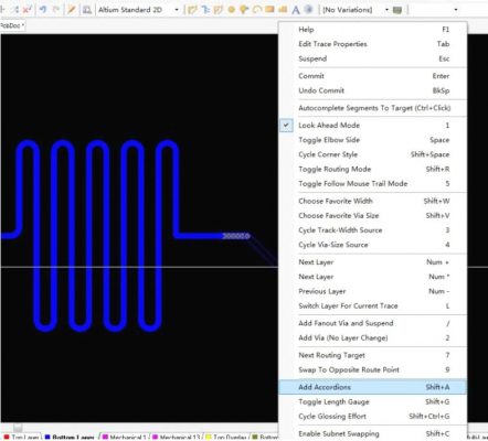
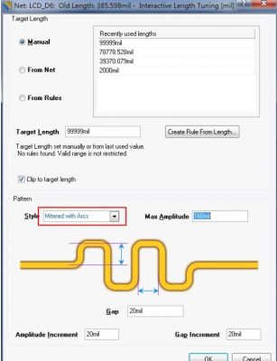
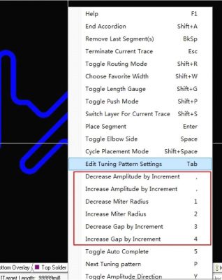
Press Tab to set the properties, type arc, Max Amplitude set the maximum amplitude, the left side below is the amplitude increment, and the right side is the gap increment.
Then start routing.
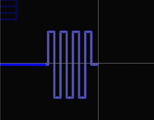
Make the edge “circle” – press the shortcut key “2”, it will increase the radius of the arc, and the maximum increase is that two 1/4 arcs are directly connected to a 180-degree semicircle. Shortcut keys “,” “.” Amplitude can be adjusted.
If you don’t remember the shortcut key, it doesn’t matter, you can press “`” at any time to display the currently supported operations.
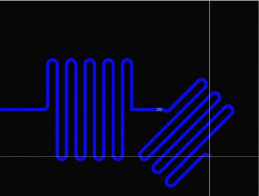
You can see the length of the network, and there is more than one place.
Equal lengths routing can be accomplished using adjusters.
Special Trace 2– Removing The Soldering Layer In The High Current Trace
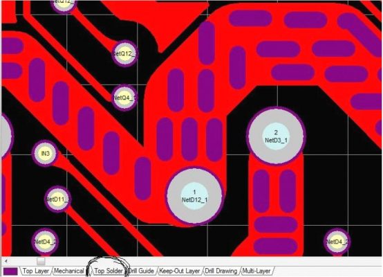
Two points need pay attention to here: First of all, the Paste layer is the real tin spray layer, but there is a solder mask layer on the default trace, so it is useless to use Paste alone, so you need to use Solder, which is marked out in this layer. There is no solder mask for the part of the tin, so the Paste+Solder method can be used to achieve the drawing of the tin spraying line. If there are traces on the board, you can directly use the Solder of the corresponding layer to open the window.
Special Trace 3– Bus Drawing
Altium Designer supports the simultaneous routing of multiple nets, and the routing can start from the pad or the beginning of the trace. Hold down the shift key to select multiple nets, or use the mouse to select multiple nets, select the menu command PLACE>>Interactive Multi-Routing and then click the bus routing tool on the routing toolbar to start the bus routing, and during the PCB routing process, you can Place vias, switch trace layers, and press commas, and periods. Branch trace spacing can be adjusted.
During the period, press 2 to add vias, and L to change layers.
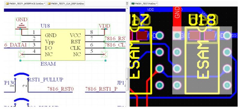
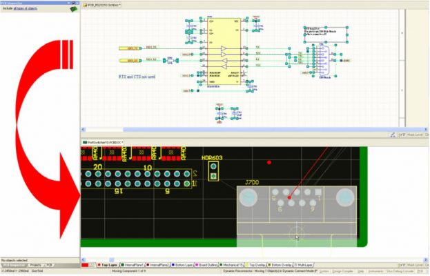
Special Trace 4– From Schematic To PCB
In the schematic, use the mouse to frame a circuit or select several devices, and press T—>S to switch to the PCB immediately and select those devices synchronously.
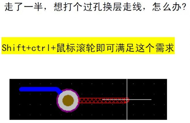
Special Trace 5– Change Layers, Operate Vias & Operate Trace In Routing
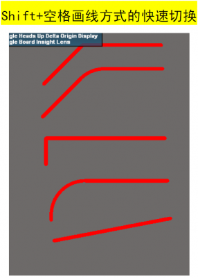
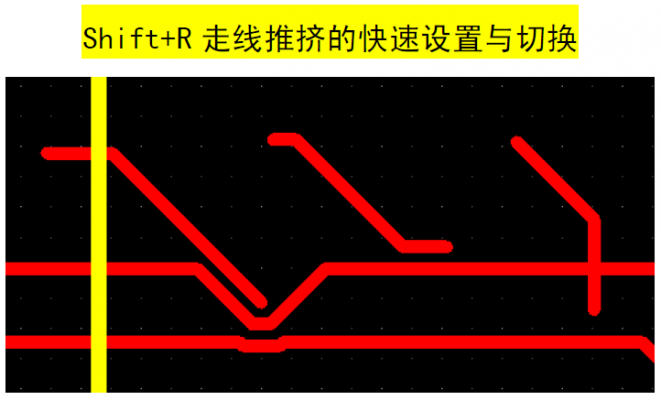
Special Trace 6– Quick Setting of Routing Push & Connection Method
Special Trace 7– Simple PCB Windows Metafile (wmf) Paste
Metafile paste makes the generation of mechanical layer design documents easier to complete. Any metafile from the clipboard can be pasted into the PCB editor by using the same Windows paste command (Ctrl+V). Metafiles can be lines, arcs, simple fills, and True Type text, and any imported data will be placed on the current layer.
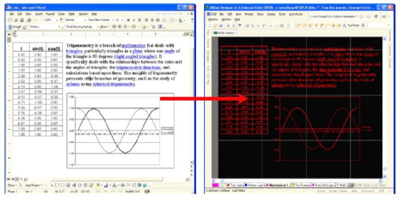
Copy data from Word or Excel to PCB. Supported metafiles include bitmaps, lines, arcs, simple fills and true type text, allowing you to easily paste logos and other graphics.
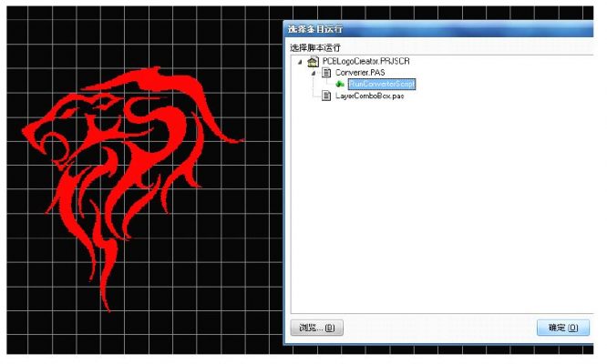
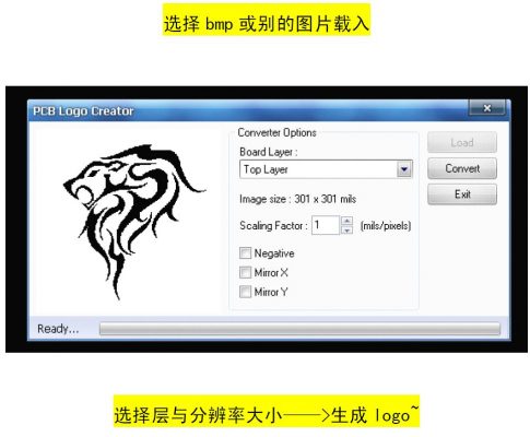
Special Trace 8– Complex Windows Metafile (wmf) Making (Like Logo)
Special Trace 9– Grid Setup and Capture
Visual grids and electrical grids in Altium Designer can be set in multiples of the capture grid (Design>>Board Options).