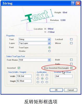
Special Trace 10– Inverse Color Output & Position Setting of Silkscreen Text
A new Valid String property box option has been added to the PCB editor. The new option can define a different rectangular bounding range for inverted text using TrueType fonts, instead of using the bounds of the inverted text itself as before.
Invert size (width/height): Set the width and height of the inverted text rectangle
Layout: Define the relative position of the text in the text box
Offset of the reversed text: Define the offset of the reversed text relative to the rectangular box
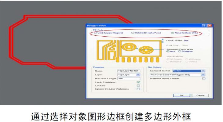
Special Trace 11– Various Polygon Area Filling
Using the Define Polygon Shape by Selection feature makes it very easy to create company logos or polygons from external sources such as DXF, Auto CAD, etc. The definition of the polygon shape is divided into two steps: first define the polygon area from the menu Tools>>Polygon Pours>>Define From selected objects, then right-click the polygon fill area and select the ‘Properties’ option from the pop-up menu, you can set the fill mode in the dialog box.
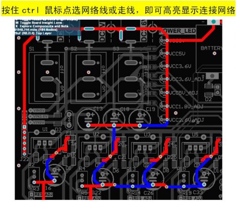
Special Trace 12– Highlight The Selected Network In The PCB
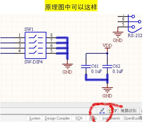
Special Trace 13– Single Layer Operation & Custom Operation
For the chaotic device layout, it is already very troublesome. If you want to route in the chaos, it is not easy. You can use shift+s in AD to solve this problem (in the PCB editing state):
In addition, I learned the customization method from the Internet, which is troublesome at first, but it will be very practical after learning.
the way is:
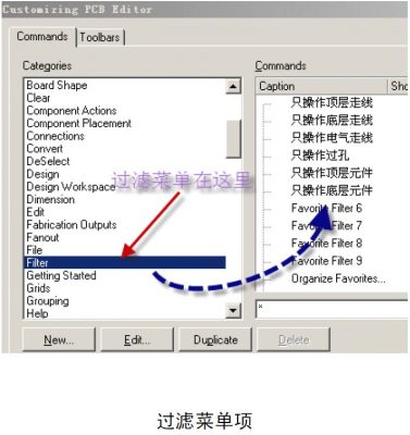
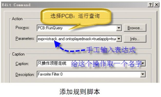
The expression that only operates the top-level trace is: expr=IsTrackandOnTopLayer|mask=True|apply=True
The expression that only operates the bottom trace is: expr=IsTrackandOnBottomLayer|mask=True|apply=True
The expression that only operates on electrical traces is: expr=IsTrackandIsElectrical|mask=True|apply=True
The expression that only operates vias is: expr=IsVia|mask=True|apply=True
The expression that only operates on top-level components is: expr=IsComponentandOnTopLayer|mask=True|apply=True
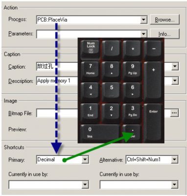
Customize several sizes of via holes, use the numeric keys in the keypad area as shortcut keys, 3 means via holes with 0.3 aperture, 4 means shortcut keys with 0.4 aperture 5…………, so you want to use any size via The holes can be easily adjusted out. I know that Altium Designer itself can use the shortcut key “shift+v” to call the vias of various sizes you filled in during the routing process, but I place the vias separately. If you want to change the size, you need to press the Tab key and rewrite the vias The size data is very troublesome. Use the following method instead:
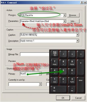
Originally, Altium used the shortcut key “P” + “V” to place vias by default. Now I use the “.” in the keypad area to achieve the same function:
Special Trace 14– Operation of Multilayer Traces
Some people ask how a line like this is drawn:
A: It is drawn one by one.
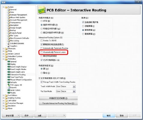
How can I set the lines to overlap? Preferences, PCB Editor, Interactive Routing, Interactive Routing Options, Automatically Remove Loops options can be canceled.
If you don’t rout one by one, you can, Place-Region, just put a polygon area, but be careful, you won’t add the network yourself. will turn green.
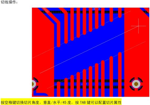
Special Trace 15– Operation of Trace Slicing
Special Trace 16– Setting & Routing of Differential Lines
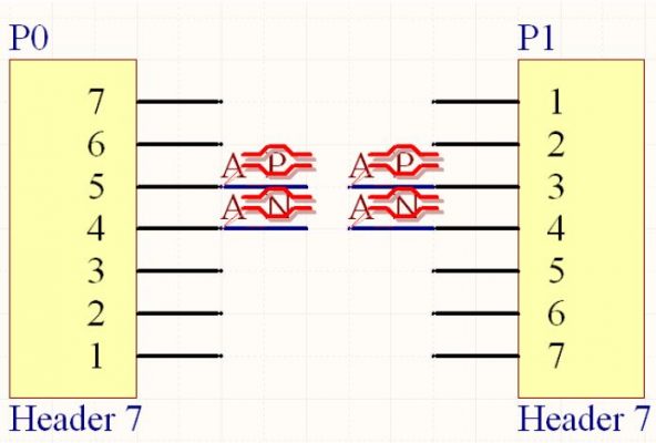
Many novices will hear “differential lines”. In fact, it is not difficult to talk about differential lines, it is just the way of wiring. Compared with the isometric lines mentioned before, it is much easier, but there are certain rules for setting:
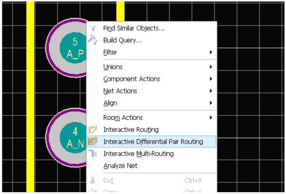
Place components and draw differential pair signals. The naming rule for differential pairs is that the names are the same, and the suffixes are marked with _P and _N respectively. Then select Place\directives\differential pairs and place the differential pair symbol.
After updating to PCB
Special Trace 17– 3D Display Operation
Your main window can be displayed in both 2D and 3D. Switch between 2D and 3D with the shortcut ‘3’ to switch from one 2D view to the previous 3D view; press ‘0’ to flatten. Shift+right+click+drag rotates your 3D view.
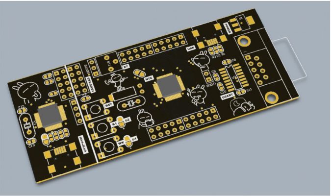
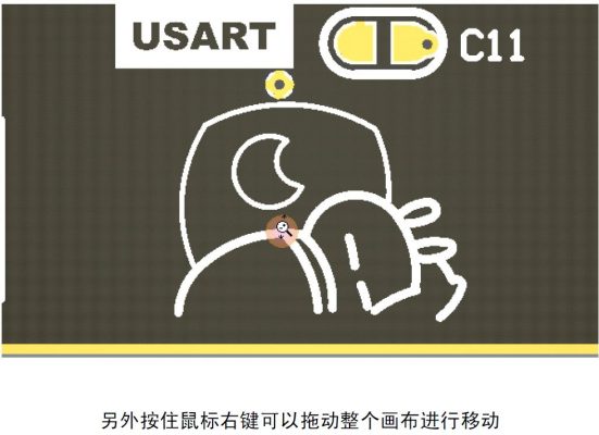
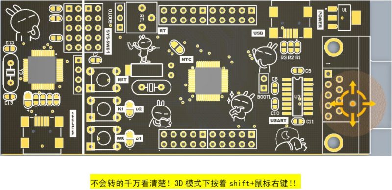
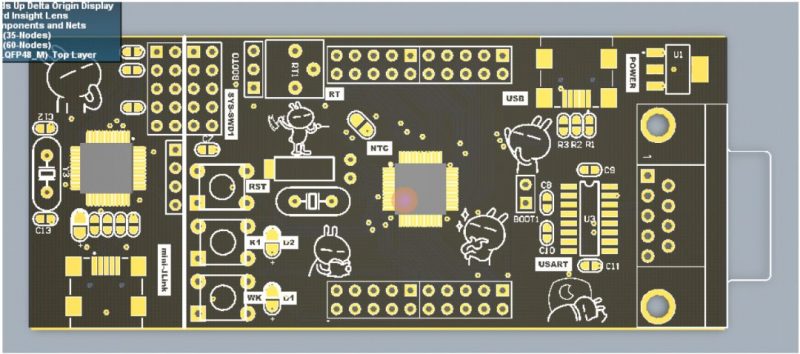
Show the newly designed board here~STM32F103C8 small board with JLINK emulator;
Special Trace 18– Quickly Zoom In & Zoom Out
There are many ways to enlarge the window, and there are only three that are really practical. The following are the introductions:
1.Full interface view
2.Ctrl+wheel (the mouse center is the center to zoom in and out)
3.Press and hold the scroll wheel for a long time to change into a magnifying glass shape, drag the mouse back and forth to quickly zoom in and zoom out.