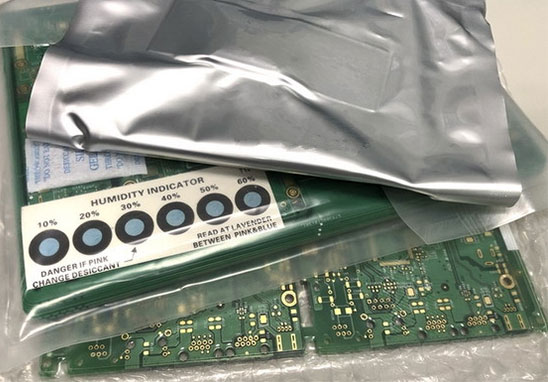
Each single process has its own inspection standards, and PCB Circuit Boards are no exception. As the core process in electronic equipment, there are many and strict inspection standards for PCB circuit boards, and the calculation of warpage is one of them.
Warpage Calculation Method of PCB
Warpage, as the name indicates, is whether the PCB printed board is flat and whether it can be perfectly inserted into the holes and surface mount pads of the board.
Warpage usually refers to the distortion of the surface of the plastic part that is not formed according to the design shape. There are plenty of factors that affect the warpage, so we must pay attention to it during production. After all, every slight error may make the whole circuit board scrapped. So how to calculate the warpage of the PCB?
Calculation formula of warpage degree of Printed Circuit Board (PCB):
Warpage = Single Corner Warp Height / (PCB Diagonal Length * 2) * 100%
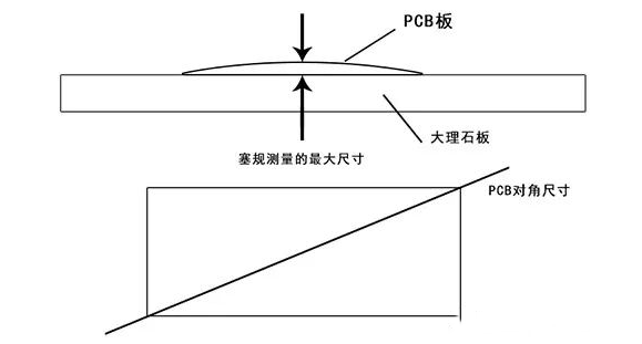
In the automatic insertion line, if the printed board is not flat, it will cause inaccurate positioning and even crash the automatic insertion machine. If the board is bent after the components are soldered, which is super difficult to cut the component feet neatly, which will eventually cause the PCB circuit board unable to be installed in the chassis or the socket in the machine, which is equivalent to scrapping a piece of circuit board. It can be seen that if the manufacturer encounters the warpage of the circuit board, it is a distressing thing, this is also why the requirements for the warpage of the PCB circuit board are becoming more and more strict.
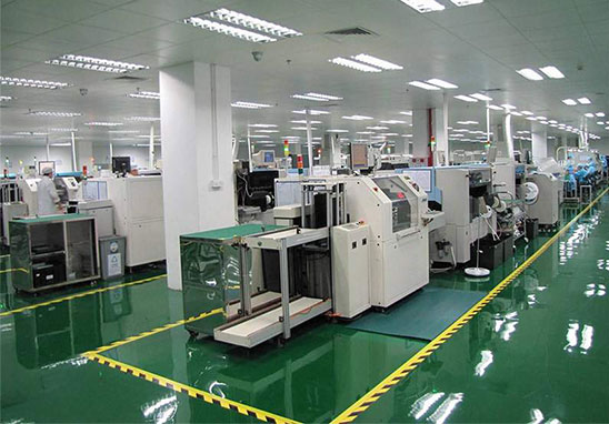
Grande PCB Production Capacity
Mass Production: 2 to 14 layers; Sample Production: 14-22 layers
Minimum Trace Width/Spacing: 3mil/3mil BGA Spacing: 0.20MM
Minimum Aperture of Finished Product: 0.1mm Size: 610mm*1200mm
Solder Mask (Ink): Japan Tamura, Taiyo, Futoken;
FR4: Shengyi, Kingboard, Haigang, Hongren, Guoji, Hazens, South Asia,
(Shengyi S1130/S1141/S1170), Tg130℃/ Tg170℃ Tg180℃ and other high TG plates)
High Frequency Board: Rogers (Rogers), Taconic, ARLLON;
Surface Finish Technology: Spray tin, lead-free spray tin, immersion gold (ENIG), full board gold plating, plug gold plating, full board thick gold, chemical immersion tin (silver), anti-oxidation (OSP) blue glue, carbon oil
Advantages Grande Circuit Board Assembly
1)Strength Guarantee
▪ SMT factory: With imported SMT machines and multiple optical inspection equipment, which is able to produce 4 million points per day. Each process is equipped with QC personnel who will keep an eye on product quality.
▪ DIP production line: Two wave soldering machines and more than 10 employees who have worked for over three years. That’ s to say, these workers are highly skilled and can weld various SMT & DIP components.
2)Quality Assurance With High Cost Performance
▪ High-end equipment can paste precision special-shaped parts, BGA, QFN, 0201 package. It can also be soldered prototype pcba via SMT machine and placing bulk materials by hand.
▪ Both samples, small and large batches can be produced. And there is no SMT Machine starting cost.
3)Rich Electronic Products SMT Soldering Experience With Stable Delivery
▪ Accumulated services to thousands of electronics companies, involving SMT soldering services for various types of automotive equipment and industrial control motherboards. Furthermore, PCBA Products are often exported to Europe and the United States, and the quality is able to be affirmed by new and regular customers.
4)Strong Maintenance Ability & Reliable After-Sales Service
▪ The maintenance engineers have sophisticated experience so that those defective boards caused by all kinds of smt soldering can be repaired. Meanwhile, ensuring the connectivity rate of each circuit board also make sense.
▪Order problems feedback will get response, solution and solved as soon as possible.