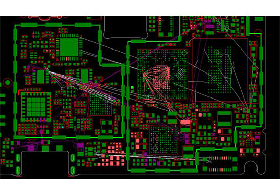
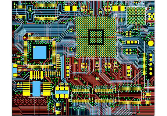
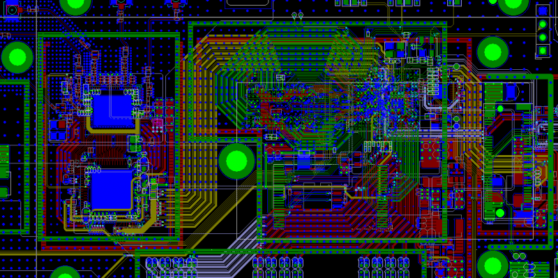
Grande is a PCB design company specializing in electronic product Circuit Board Design (PCB Layout). It mainly undertakes multi-layer, high-density PCB design drawing boards and circuit board design proofing business. Now, let’s see the common problems in PCB design.

1.Pads Overlap
1)Overlapping of pads means overlapping of holes due to bit breakage and hole damage caused by drilling multiple holes in one location during the drilling process.
2)The two holes on the multilayer board overlap.
2.The Abuse of The Graphics Layer
1)Some useless connections are made on some graphics layers.
2)PCB design requires fewer traces.
3)Violating the traditional design, such as the component surface is designed on the bottom layer and the soldering surface is designed on the top layer, causing inconvenience.
3.Random Placement of Characters
1)The SMD pad of the character cover brings inconvenience to the on-off test of the circuit board and the soldering of components.
2)The character design is too small, making screen printing difficult. Too large will cause the characters to overlap and be difficult to distinguish.
4.The Setting of The Single Pad Aperture
1)Single-sided pads are usually not drilled. If the drill hole need to be marked, the hole diameter should be designed to be zero.
2)Single-sided pads should be specially marked if drilled.
5. Artboards With Filler Blocks
When solder resist is applied, the fill block area will be covered with solder resist, making components soldering difficult.
6.The Formation of Electricity is Flower Pad Connection
Because the power supply is designed in a flower pad pattern, the ground plane is opposite the image on the actual printed circuit board, and all connecting tracees are isolated. When routing isolation traces for several sets of power supplies or several types of grounds, no gaps should be left to short out the two sets of power supplies or block the connection area.
7. The Definition of Assembly Grade is Not Clear
1)The single board is designed on the top layer. If the front and back are not stated, the panel may be fabricated with components mounted, not soldered.
2)When designing a four-layer board, use the top, middle 1 and middle 2 layers, and bottom 4 layers, but they are not arranged in this order during Assembly.
8. Too Many Filling Blocks In The PCB Design Or The Filling Blocks Are Filled With Extremely Thin Traces
1)There is data loss in the light drawing, and the data is incomplete.
2)Since the filling block is drawn line by line during the light drawing data processing, the amount of data generated is quite large, which increases the difficulty of data processing.
9. The Surface Mount Component Pad is Too Short
For surface mount components that are too dense, a staggered top-to-bottom (left-to-right) position must be used in order to mount the test pins.
10. Large Area Grid Spacing is Too Small
The edges between the same traces that make up the large-area grid lines are too small (less than 0.3 mm), and many broken films are easily attached to the circuit board after the image is displayed, resulting in broken traces.
11. Large Area Copper Foil is Too Close To The Outer Frame
The distance between the large area copper foil and the outer frame should be at least 0.2 mm.
12. The Outline Frame Design is Not Clear
Some customers have contours designed on reserved layers, board layers, top layers, making it difficult for board manufacturers to determine which contour should prevail.
13.The Graphic Design is Not Unified
When the pattern is electroplated, the uneven coating will affect the quality.
14. Special-Shaped Hole is Too Short
The length/width of the special-shaped hole should be ≥ 2: 1, and the width should be greater than 1.0 mm, otherwise the drilling machine is easy to break during processing, processing is difficult, and the cost is increased.
Grande PCB Layout Capability
Maximum Signal Design Rate: 10Gbps CML differential signal;
Maximum PCB Design Layers: 40 layers;
Minimum Trace Width: 2.4mil;
Minimum Trace Spacing: 2.4mil;
Minimum BGA PIN Spacing: 0.4mm;
Minimum Mechanical Hole Diameter: 6mil;
Minimum Laser Drilling Diameter: 4mil;
Maximum Number of PINs: ;63000+
Maximum Number of Components: 3600;
Maximum Number of BGAs: 48+.