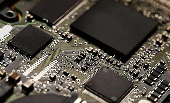
In PCB Assembly, SMD and DIP components are usually used. So, what is the difference between SMD & DIP components?
The Difference Between SMD and DIP Components
1.Appearance Difference
1)SMD components are small in size, light in weight, and easier to solder than DIP components.
2)SMD components have a super important advantage, that it to improve the stability and reliability of the circuit; Mainly because the SMD components have no leads, stray electric fields and magnetic fields are reduced, which is effective especially obvious in high-frequency analog circuits and high-speed digital circuits.
2.Soldering Method Difference
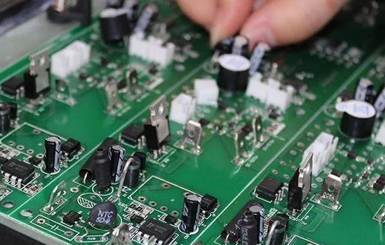
1)Soldering method of SMD components: Put the components on the pad, apply the adjusted SMD solder paste on the surface of the component and the contact of the pad, and then use a 20W internal heating electric soldering iron to the pad and SMD components, heat the connection (the temperature should be 220~230℃), and the soldering iron can be removed after seeing the melting of the solder, and the soldering is completed after the solder solidifies. After soldering, you can use tweezers to clamp the soldered SMD components to see if there is any looseness. If there is no looseness, it means that the soldering is good.
2)Soldering method of DIP components: When soldering all pins, solder should be added to the tip of the soldering iron, and all pins should be coated with flux to keep the pins wet. Touch the end of each pin of the chip with the tip of the soldering iron until the solder flows into the pin. After soldering all the pins, wet the pins with flux to clean the solder to remove any shorts and laps. Finally, use tweezers to check whether there is any virtual soldering. After the inspection is completed, remove the flux from the circuit board, and dip a bristle brush in alcohol and wipe it carefully along the direction of the pins until the flux disappears.
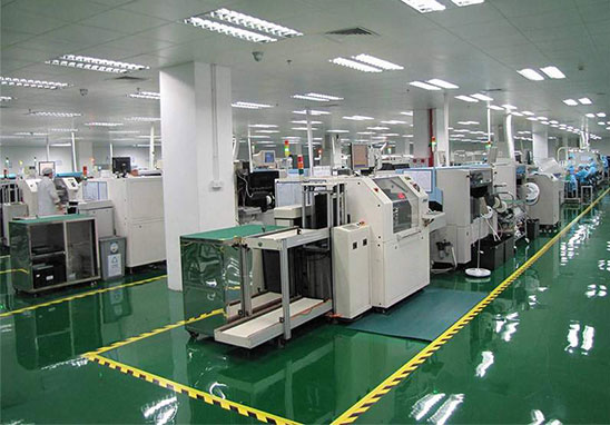
Grande PCBA Advantages
1. Highly Professional: Focus on PCBA Sample, small and medium batches, and promises to deliver within 3-5 working days after the materials are confirmed to be correct.
2. Professional Equipment: Advanced equipment tailored for sample and small and medium batch production, and can be pasted with 0201, BGA spacing 0.3MM, QFN, CSP, CON and other components.
3. Professional Technology: 100% of technical backbones have more than 5 years of work experience, and 85% of front-line operators have more than 3 years of work experience.
4. The company implements the 5S and 6σ concepts in daily operations, and it is expected that the shipment will be checked at least 7 times. Promise to pass AOI optical inspection if the quantity reaches 100PCS.
5. Guarantee the soldering pass rate is above 99%. If the customer finds soldering defects, Grande promises to repair it for free immediately.