In PCB design, after completing the circuit board design through many levels, the most important issue is the copyright issue, and plagiarism is not uncommon. So, how to prevent others from copying board in PCB design?
The Methods of Anti-Copying In PCB Design
1. Grinding, use fine sandpaper to grind off the model on the chip; And it is more effective for rare chips.
2. Brushing potting material, to cover all the components on the PCB; Five or six flying wires can also be deliberately screwed together. It is important to note that the potting material cannot corrode and the heat in the enclosed area will not be too great.
3. Use dedicated encryption chips, such as ATMEL’s AT88SC153.
4. Use unbreakable chips, such as unbreakable chips, EPLD’s EPM7128 or above, ACTEL’s CPLD, etc.
5. Use MASKIC, which requires a lot of batches.
6. With bare chips, plagiarists can’t see the model number or know the wiring. Pay attention to, the function of the chip should not be too easy to guess.
7. Connect a resistor of more than 60 ohms in series on the signal line with low current.
8. Use some small components without words (or only some codes) to participate in signal processing, such as small chip capacitors, TO-XX diodes, etc.
9. Cross some address and data lines.
10. The PCB adopts buried via and blind via technology, so that the via hole is hidden in the board.
11. Use other special accessories, such as custom LCD screen, custom transformer, etc.
12. Apply for a patent. In view of the poor environment for intellectual property protection, the best method abroad can only be placed in the last one.
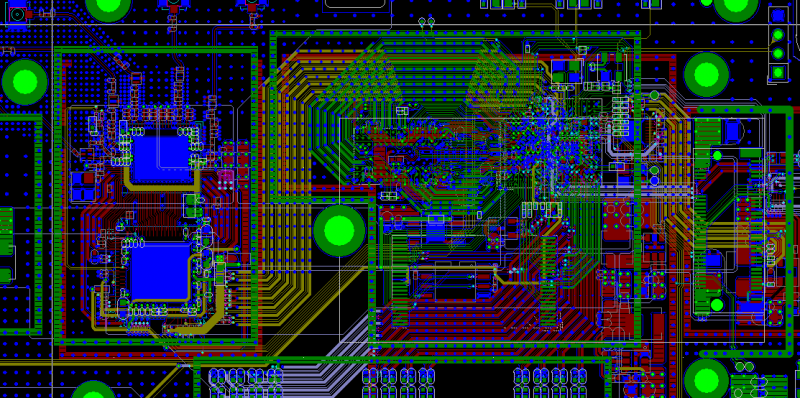
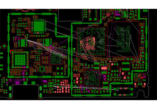
Grande PCB Design Capability
The Highest Signal Design Speed: 10Gbps CML differential signal;
Maximum PCB Design Layers: 40 layers;
Minimum Line Width: 2.4mil;
Minimum Line Spacing: 2.4mil;
Minimum BGA PIN Spacing: 0.4mm;
Minimum Mechanical Hole Diameter: 6mil;
Minimum Laser Drilling Diameter: 4mil;
Maximum Number of PINs: ;63000+
Maximum Number of Components: 3600;
Maximum Number of BGAs: 48+.
PCB Design Service Process
1. Customers provide schematic to consult PCB design;
2. Grande evaluates the quotation in the light of the schematic and customer design requirements;
3. The customer confirms the quotation, signs the contract, and prepays the project deposit;
4. Grande receives advance payment and arranges PCB Layout engineer to design;
5. After the PCB Layout is completed, Grande provides a screenshot of the document to the customer for confirmation;
6. The customer confirms OK, settles the balance, and provides PCB design information.