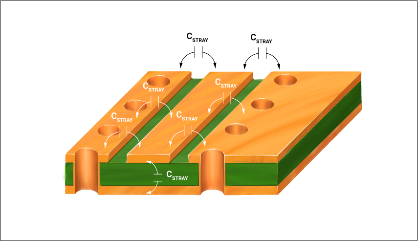
When referring to electronic circuits on the PCBA, a term often used is stray capacitance. Stray capacitance can exist between conductors on PCBs, prefabricated circuit boards for passive components, PCBA, between boards with mounted components, and between SMD component kits in component packages (especially ICs). Stray capacitance is one of the physical properties inherent in electronic circuits and circuit boards. So how to reduce the impact of PCB stray capacitance?
Reduce PCB Stray Capacitance By PCB Design
1. Remove the inner ground plane
Since ground planes can increase capacitance with adjacent conductors due to their proximity, it helps to remove inner ground planes to increase the distance, which will minimize capacitive effects. This must be weighed against the benefit of minimizing the EMI gained when the ground plane is adjacent to the signal plane.
2. Use the Faraday Shield
A Faraday shield is a ground trace or plane that is placed between two traces, the PCB is designed to minimize capacitive effects between them, and like other shielding structures, it effectively reduces stray capacitance.
3. Increase the space between adjacent traces
Another effective mitigation technique is to increase the spacing between adjacent traces. This is a quite good method to apply as capacitance decreases with distance.
4. Minimize the use of vias
Through holes are a key element in making compact, complex PCBs possible. However, overuse may increase parasitic capacitance problems. Such as stray capacitance. This PTH coupling can be reduced by PCB design eliminating annular rings around vias on unconnected layers and minimizing the number of vias from components. Such as BGA.
Grande Electronic Circuit Board Design Capabilities
Maximum signal design rate: 10Gbps CML differential signal
Maximum PCB design layers: 40 layers
Minimum trace width: 2.4mil
Minimum trace spacing: 2.4mil
Minimum BGA PIN spacing: 0.4mm
Minimum mechanical hole diameter: 6mil
Minimum laser drilling diameter: 4mil
Maximum number of PINs: 63000+
Maximum number of components: 3600
Maximum number of BGAs: 48+
Grande PCB Assembly Advantages
1)Strength Guarantee
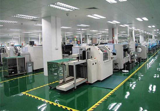
 SMT factory: With imported SMT machines and multiple optical inspection equipment, which is able to produce 4 million points per day. Each process is equipped with QC personnel who will keep an eye on product quality.
DIP production line: Two wave soldering machines and more than 10 employees who have worked for over three years. That’ s to say, these workers are highly skilled and can weld various SMT & DIP components.
2)Quality Assurance With High Cost Performance
High-end equipment can paste precision special-shaped parts, BGA, QFN, 0201 package. It can also be soldered prototype pcba via SMT machine and placing bulk materials by hand.
Both samples, small and large batches can be produced. And there is no SMT Machine starting cost.
3)Rich Electronic Products SMT Soldering Experience With Stable Delivery
Accumulated services to thousands of electronics companies, involving SMT soldering services for various types of automotive equipment and industrial control motherboards. Furthermore,PCBA Products are often exported to Europe and the United States, and the quality is able to be affirmed by new and regular customers.
4)Strong Maintenance Ability & Reliable After-Sales Service
The maintenance engineers have sophisticated experience so that those defective boards caused by all kinds of smt soldering can be repaired. Meanwhile, ensuring the connectivity rate of each circuit board also make sense.
Order problems feedback will get response, solution and solved as soon as possible.