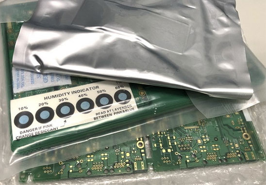
Which inspections are required for PCB bare board before shipping? Many customers are concerned about this question. PCB bare board need undergo multiple inspections, and can only be shipped after a shipment inspection report is issued.
1. Basic Inspection
Laminate Information: Type, Finished Board Thickness, Outer Copper Foil, Inner Copper Foil, Warpage, Ink, Color, Position, Marking, Minimum Trace Width, Spacing, Ring Width, Solder Mask, Surface Finishing, Special Process, Test Items, Films, etc.
2. Electrical Performance Test Report
1)Test Category: Single-sided, general-purpose, special-purpose, number of test points.
2)Test Parameters: Current, voltage, on-resistance, insulation voltage, etc.
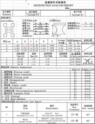
3. Metallographic Section Analysis Report
Copper thickness, nickel thickness, gold thickness, lead-tin thickness, copper thickness of circuit, roughness, etching factor, coating crack, resin shrinkage, coating void, delamination, etc.
4. Impedance Test
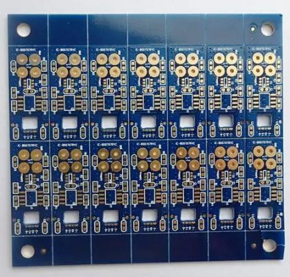
Grande PCB Capability
Mass production 2 to 14 layers, Sample 14-22 layers;
Minimum line width/spacing: 3mil/3mil BGA spacing: 0.20MM
Minimum aperture of finished product: 0.1mm Size: 610mmX1200mm
Ink: Japan Tamura, Taiyo, Futoken;
FR4: Shengyi, Kingboard, Haigang, Hongren, Guoji, Hazens, South Asia,
(Shengyi S1130/S1141/S1170), Tg130℃/ Tg170℃ Tg180℃ and other high TG plates)
High frequency board: Rogers (Rogers), Taconic, ARLLON;
Surface technology: spray tin, lead-free spray tin, immersion gold, full board gold plating, plug gold plating, full board thick gold, chemical immersion tin (silver), anti-oxidation (OSP) blue glue, carbon oil
Lead Time of Fast PCB Prototype
Double-sided board can be completed within 24 hours, and multi-layer pcb can be completed within 2-5 days;
Single/double-sided board (0.6-1.6mm FR4) lead time: 3-4 days;
Four-layer board (0.6-1.6mm FR4) delivery time: 5-6 days;
Six-layer board (0.8-1.6mm FR4) lead time: 7-8 days.