A good PCB laminate design is essential to reduce the radiation of PCB loops and related circuits. On the contrary, bad laminate design may significantly increase radiation, which is harmful from a safety point of view.
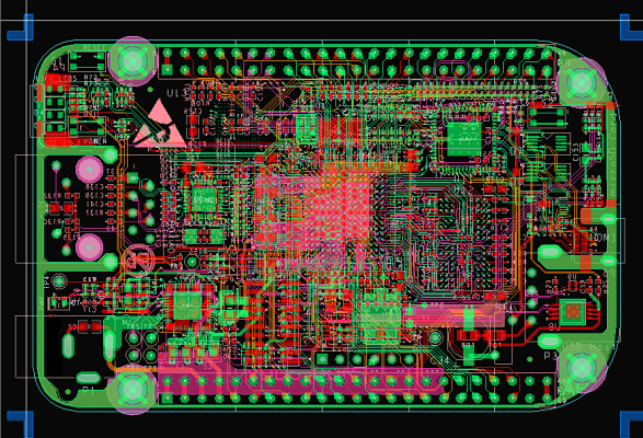
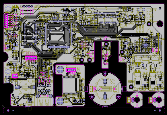
There are many different multilayer circuit board designs in PCB laminate technology. When multiple layers are involved, a three-dimensional approach that considers the internal structure and surface layout must be combined. With the high operating speed of modern circuits, careful PCB laminate design must be done to improve the distribution capability and limit interference. A poorly designed PCB may reduce signal transmission, productivity, power transmission and long-term reliability.

What is PCB Laminate?
Before the final layout design is completed, the PCB laminate layers the insulator and copper of the PCB. Developing effective laminate is a complex process. PCB connects power and signals between physical devices, and the correct layering of circuit board materials directly affects its function.
Why do we need PCB laminate?
The development of PCB laminate is essential for designing efficient circuit boards. By and large, PCB laminate has a number of benefits, such as the multilayer structure can improve energy distribution, prevent electromagnetic interference, limit cross interference, support high-speed signal transmission and so on.
Although the main purpose of laminate is to place multiple electronic circuits on one board through multiple layers, we can’t deny that the laminate structure of PCBs also provides other important advantages. These measures include minimizing the vulnerability of circuit boards to external noise and reducing crosstalk and impedance problems in high-speed systems.
Apart from than, a good PCB laminate can also help ensure lower final production costs. By maximizing efficiency and improving the electromagnetic compatibility of the entire project; In a nutshell, PCB laminate can effectively save time and money.
Precautions & Rules For PCB Laminate Design
1) Number of layers
Simple laminate may include four-layer PCBs, while more complex boards require professional sequential lamination. Although more complex, the higher number of layers allows designers to have more layout space without increasing the risk of encountering impossible solutions.
Generally, eight or more layers are required to obtain the best layer arrangement and spacing to maximize functionality. Using quality planes and power planes on multilayer boards can also reduce radiation.
2) Layer arrangement
The arrangement of the copper layer and the insulating layer constituting the circuit constitutes the PCB overlap operation. To prevent PCB warping, it is quite necessary to make the cross section of the board symmetrical and balanced when laying out the layers. For instance, in an eight-layer board, the thickness of the second and seventh layers should be similar to achieve the best balance.
The signal layer should always be adjacent to the plane, while the power plane and quality plane are strictly coupled together. It is best to use multiple ground planes, because they generally reduce radiation and lower ground impedance.
3) Layer material type
The thermal, mechanical, and electrical properties of each substrate and how they interact are critical to the choice of PCB laminate materials.
The circuit board is usually composed of a strong glass fiber substrate core, which provides the thickness and rigidity of the PCB. Some flexible PCBs may be made of flexible high-temperature plastics.
The surface layer is a thin foil made of copper foil attached to the board. Copper is present on both sides of a double-sided PCB, and the thickness of the copper varies according to the number of layers of the PCB stack.
Cover the top of the copper foil with a solder mask to make the copper traces contact other metals. This material is essential to help users avoid soldering the correct location of jumper wires.
A screen printing layer is applied on the solder mask to add symbols, numbers and letters to facilitate assembly and allow people to better understand the circuit board.
4) Determine wiring and through holes
Designers should route high-speed signals on the middle layer between layers. This allows the ground plane to provide shielding that contains radiation emitted from the track at high speeds.
The placement of the signal level close to the plane level allows the return current to flow on the adjacent plane, thereby minimizing the return path inductance. There is not enough capacitance between adjacent power and ground planes to provide decoupling below 500 MHz using standard construction techniques.
5) Spacing between layers
Due to the reduced capacitance, tight coupling between the signal and the current return plane is critical. The power and ground planes should also be tightly coupled together.
The signal layers should always be close to each other even if they are located in adjacent planes. Tight coupling and spacing between layers is essential for uninterrupted signals and overall functionality.