PCB design is a very detailed work, so you should be very careful and patient when designing, fully consider various factors, including production assembly processing details, post-maintenance convenience, etc.. In addition, developing some good working habits in the design will make the design more reasonable, more efficient design, easier production and better performance. Good design applied to everyday products, consumers will be more assured and trust.
The basic PCB design process is as follows:
Preliminary preparation → PCB structure design → guide network table → rule setting → PCB layout → wiring → wiring optimization and screen printing → network and DRC check and structure check → output light painting → light painting review → PCB board production / proofing data → PCB board factory engineering EQ confirmation → SMD data output → project completion.
1、Pre-preparation
Including the preparation of mounting libraries and schematics. Before PCB design, first prepare the schematic logic package and PCB packaging library. The pads have their own library, but it is generally difficult to find the right one, it is best to make their own packaging library based on the standard size data of the selected device. In principle, first do the PCB packaging library, and then do schematic logic package. PCB packaging library is more demanding, directly affecting the installation of the plate. SCH logic package requirements are more relaxed, just pay attention to the definition of pin properties and correspondence with the PCB package.
Ps: pay attention to the standard library of hidden pins, followed by the design of the schematic, and then you can start to do PCB design.
This step is based on the determination of the board size and various mechanical positioning, in PCB drawing design environment PCB board surface, and according to the positioning requirements to place the required connectors, buttons / switches, screw holes, assembly holes, etc.. And fully consider and determine the wiring area and non-wiring areas (such as around the screw holes belong to the scope of non-wiring areas).
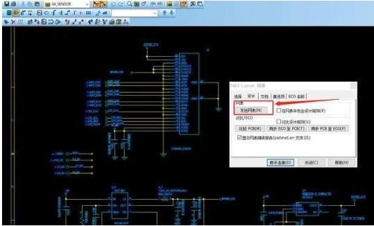
3、Guide the mesh table
It is recommended to import the frame before importing the netlist. Import the board frame in DXF format or emn format.
4、Rule setting
According to the specific PCB design reasonable rules, we are talking about the rules are PADS constraint manager through the constraint manager in any part of the design process to constrain the line width and safety spacing. DRC detection will be marked out using DRC Markers.
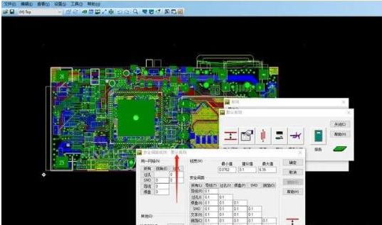
Generally the rule setting is placed before the layout, because sometimes the layout has to finish some fanout work, so the rule should be set before the fanout, when the design project is larger, it can finish the design more efficiently.
Note: Setting rules is to complete the design better and faster, in other words, to facilitate the designer.
The general settings are.
Default line width/line spacing 1. Normal signal.
- Select and set the over-hole
- Line width and color settings for important signals and power supplies.
- Board layer settings.
5、PCB layout
General layout according to the following principles.
(1) according to the electrical performance of a reasonable partition, generally divided into: digital circuit area (i.e., fear of interference, fear of interference), analog circuit area (fear of interference), power drive area (interference sources).
(2) Circuits to accomplish the same function should be placed as close as possible, and adjust the components to ensure the simplest connection; adjust the relative position between the functional blocks to make the simplest connection between the functional blocks.
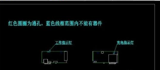
(3) High-quality components should be considered for installation location and strength; heating elements should be placed separately from temperature-sensitive components, and thermal convection measures should be considered when necessary.
(4) I/O driver devices as close as possible to the edge of the printed board, close to the lead-in connector.
(5) clock generator (such as crystal or clock oscillator) should be as close as possible to the device using the clock.
(6) in each integrated circuit between the power input pin and the ground to increase the decoupling capacitor (generally using high-frequency monolithic capacitors); when the board space is dense, you can also add tantalum capacitors around several integrated circuits.
(7) relay coils should be added to the discharge diode (1) N4148 can be).
(8) the layout requires a balanced, orderly density, head-heavy or head-heavy
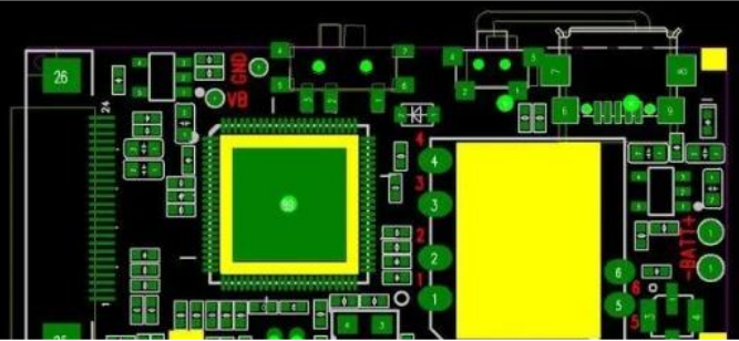
Special attention needs to be paid to the placement of components, must take into account the actual size of components (area and height) and the relative position between components to ensure the electrical performance of the board and the feasibility and convenience of production and installation. At the same time, in order to ensure that the above principles can be reflected in the premise, the placement of equipment should be appropriately modified to make it neat and beautiful, the same equipment should be placed neatly and in the same direction, not placed “staggered”.
This step is related to the overall image of the board and the difficulty of the next wiring, so it needs to be strongly considered. When laying out the board, the initial wiring can be done in uncertain places with full consideration.
6、Wiring
Cabling is the most important design process for the entire PCB. This will directly affect the design. PCB board performance is good or bad PCB in the design process, wiring generally has three realms.
The first is the cloth through, the most basic requirements of the PCB design at this time. If the line is not laid through, there are flying lines everywhere, it will be a substandard board, so to speak, has not yet begun.
The second is to meet the electrical performance. This is a measure of whether the printed circuit board is qualified. This is wiring after careful adjustment of the wiring to achieve the best electrical performance.
Then there is beauty. If your wiring is connected, there is nothing to affect the electrical performance, but at a glance it looks disorganized, colorful and colorful, even if your electrical performance is good, it is garbage in the eyes of others. This brings great inconvenience to testing and maintenance. The wiring should be neat and tidy, not crisscrossed. These should be achieved while ensuring the performance of the appliance and meeting other personal requirements, otherwise it is to put the cart before the horse.
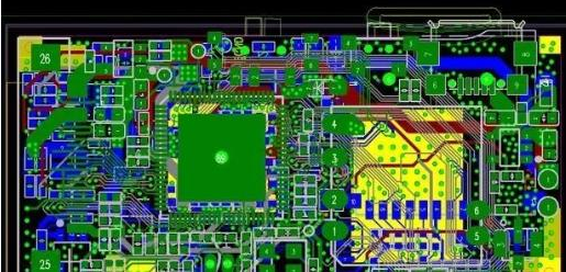
Wiring is done mainly according to the following principles:
(1) In general, the power and ground lines should be wired first to ensure the electrical performance of the board. Within the limits of the conditions, try to widen the power and ground line width, preferably wider than the power line. The relationship between them is: ground line > power line > signal line, usually the signal line width: 0.2 to 0.3mm (about 8-12mil), the minimum width of up to 0.05 to 0.07mm (2-3mil), the power line is generally 1.2 to 2.5mm (50-100mil). Digital circuit PCB wide ground can form a circuit, that is, constitute a ground network used (analog circuit ground can not be used in this way).
(2) advance wiring requirements of strict lines (such as high-frequency lines), the edges of the input and output should be avoided adjacent parallel to avoid reflective interference. If necessary, ground isolation should be increased, the wiring of adjacent layers should be vertical, parallel easy to produce parasitic coupling.
(3) oscillator shell ground, the clock line should be as short as possible, can not be attracted everywhere. Under the clock oscillation circuit, the area of the special high-speed logic circuit should be increased, rather than other signal lines, so that the surrounding electric field is close to zero.
(4) as far as possible to use 45 as far as possible to use ° can not use 90 fold line ° folded to reduce the radiation of high-frequency signals, folded line; (require high line also to use double arc line)
(5) any signal lines should not form loops, such as unavoidable, loops should be as small as possible; signal lines should be as small as possible over the hole;
(6) the key line as short and thick as possible, and on both sides with a protective ground.
(7) through the flat cable transmission of sensitive signals and noise field band signal, should use the “ground – signal – ground” lead out way.
(8) Key signals should be reserved for test points to facilitate production and maintenance testing
(9) After the schematic wiring is completed, the wiring should be optimized; at the same time, after the preliminary network check and preliminary network check, and at the same time, the DRC check is correct, fill the ground of the unwired area, use a large area of copper layer as ground, and connect the unused area to the printed board as ground. Or make a multilayer board with one layer each for power and ground.
7、Wiring optimization and silk screen printing
“There is no best, only better”! No matter how hard you design, go back to it after drawing, you will still feel that many places can be modified. General design experience is:Optimize the wiring twice as long as the first wiring. Feel no place to modify, and then lay copper. Copper laying generally lay the ground (note the separation of analog ground and digital ground), multilayer boards may also need to lay power. For screen printing, be careful not to get blocked by equipment or removed by vias and pads. At the same time, the design should be squarely on the surface of the component, and the text on the bottom should be mirrored to avoid confusing the level.
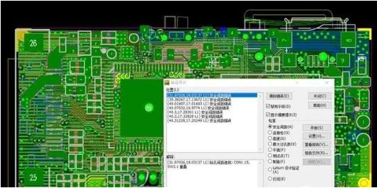
8、Network, DRC check and structure check
Before coming out of the light, generally need to check, each company will have their own CheckList, which package principle, design, production and other aspects of the requirements. The following are the two main check functions provided by the software.
DRC check.
9、Export light painting
Before light drawing output, you need to ensure that the veneer is the latest version that has been completed and meets the design requirements. The light drawing output files are used for board factory board, stencil factory stencil, welding factory process files, etc. respectively.
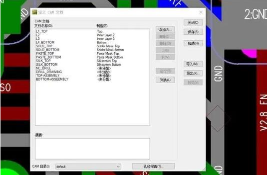
The output file includes (four-layer board as an example):
1) Wiring layer: refers to the conventional signal layer, mainly wiring.
Named L1,L2,L3,L4, where L represents the layer layer.
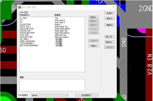
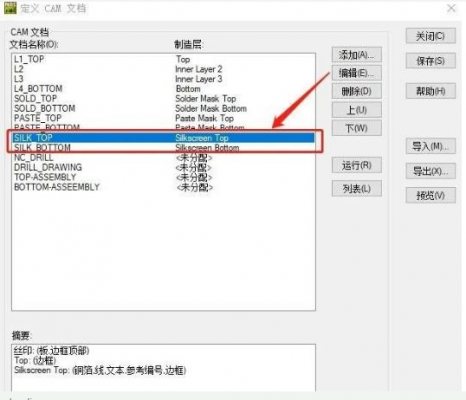
2) Screen print layer: The level of the design file that provides information for processing screen printing. Usually, when there is equipment or logo on the top and bottom layers, there will be top screen printing and bottom screen printing.
Naming: The top layer is named SILK_TOP; the bottom layer is named SILK_BOTTOM.
(3) SOLDER RESISTANCE LAYER: The level that provides processing information for green paint in the design file.
Naming: The top layer is named SOLD_TOP; the bottom layer is named SOLD_BOTTOM.
(4) Stencil layer:It refers to the level in the design document that provides processing information for the solder paste coating, and is usually found in both the top and bottom layers SMD in the device conditions, there will be a stencil top layer and a stencil bottom layer.
Naming: The top layer is named PASTE_TOP; the bottom layer is named PASTE_BOTTOM.
5) Drilling layer (including 2 files, NCDRILL CNC drilling file and DRILLDRAWING drilling map)
Named NCDRILL and DRILLDRAWING respectively.
After the output of light painting to light painting inspection, Cam350 open short circuit and other aspects of the inspection can be sent to the board factory to make the board, and later also pay attention to the production of the board engineering and problem response.