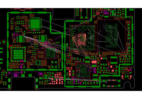
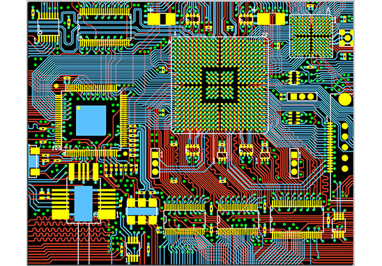
PCB design technology is kind of complex and involves many problems in lots aspects. To do a good job in PCB design requires the accumulation of experience. Grande has specialized in PCB design for more than 20 years. Now, let’s see eight common technical problems in PCB design together!
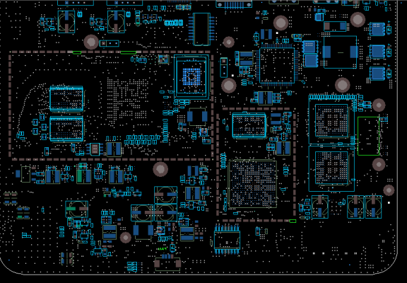
Eight Common Technical Problems of PCB Design
Q1. When designing a system containing DSP and PLD, what aspects should ESD be considered?
A1. As far as the general system is concerned, it mainly considers the part that is in direct contact with the human body, and properly protects the circuit and mechanism. As for how much ESD will affect the system, it actually depends on different situations.
Q2. In the EMC test, it was found that the harmonics of the clock signal exceeded the standard extremely seriously, just connect the decoupling capacitor to the power supply pin. What aspects should pay attention to in the design to suppress electromagnetic radiation?
A2. The three elements of EMC are the radiation source: The transmission route and the victim; The transmission route is divided into space radiation transmission and cable conduction. So to suppress harmonic wave, first look at the way it propagates. Power supply decoupling is the solution to conduction mode propagation, in addition, necessary matching and shielding are also required.
Q3. Among the products with 4-layer board design, why are some surface ground applying and some not?
A3. The role of surface ground applying: 1.Shielding; 2.Heat dissipation; 3.Reinforcement; 4.Processing needs. No matter how many layers of boards are laid, the main reason for it is to first look at it. Here we mainly discuss the high speed problem. Surface ground applying is good for EMC, but copper applying should be as complete as possible to avoid islands.
Q4. For boards with a frequency of more than 30M, use automatic routing or manual routing?
A4: Well, automatic or manual routing depends on the support of the software routing function. Some routing may be better than automatic routing, but for some routing, such as checking distribution routing, bus delay compensation routing, the effect and efficiency of automatic routing will be much higher than manual routing.
Q5. In the design, the ground wire is usually divided into protection ground and signal ground; The power ground is divided into digital ground and analog ground. Why should the ground wire be divided?
A5. The purpose of dividing the ground is mainly for the consideration of EMC. Because we worried that the noise of the power supply and ground of the digital part will interfere with other signals, especially the analog signal through the conduction path. No matter how it is divided, there is only one land in the end.
Q6. Is it necessary to shield the ground wire on both sides when laying the clock?
A6. Whether to add a shielded ground wire depends on the crosstalk /EMI situation on the board. If the shielded ground wire is not handled properly, it may make the situation worse.
Q7. What are the corresponding countermeasures for clock lines with different frequencies?
A7. For the routing of the clock line, it is best to perform signal integrity analysis, formulate corresponding routing rules, and perform routing in the light of these rules.
Q8. When the single-layer board is manually wired, how should the jumper be represented?
A8. The jumper is a special device in the design. There are only two pads. The distance can be fixed or variable. Manual routing can be added as needed. There will be a straight line on the board, and it will also appear in the bill of materials.
Grande PCB Design Capability
Maximum signal design rate: 10Gbps CML differential signal;
Maximum PCB design layers: 40 layers;
Minimum line width: 2.4mil;
Minimum line spacing: 2.4mil;
Minimum BGA PIN spacing: 0.4mm;
Minimum mechanical hole diameter: 6mil;
Minimum laser drilling diameter: 4mil;
Maximum number of PINs: ;63000+
Maximum number of components: 3600;
Maximum number of BGAs: 48+.
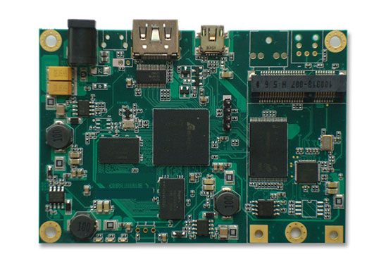
Grande is a PCB design company specializing in electronic product circuit board design (PCB Layout). It mainly undertakes multi-layer, high-density PCB design and circuit board prototype business. The PCB design team with an average of more than 10 years of work experience can proficiently use the mainstream PCB design software in the market, professional and efficient communication to ensure the progress of the PCB design as well as help you seize the market opportunities earlier!