In current PCB design, there are 5 regular disciplines, components arrangement discipline, according to the principle of signal direction layout, electromagnetic interference prevention discipline, thermal interference suppression discipline, and the layout discipline of adjustable elements.
Components Arrangement Discipline In PCB Design
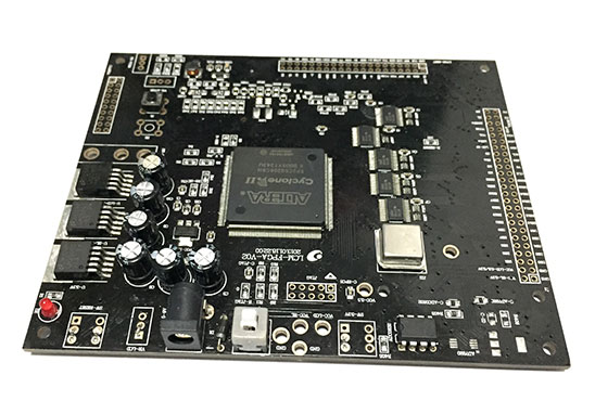
1. Under normal conditions, the owner’s original case is on the same surface as the inscription control circuit, and the original case is overcrowded. , 贴 IC, etc.
2. Under the premise of the performance of the electricity in the insurance, the original case is left unattended and parallel or vertical arrangement, and the ordering, beauty, general situation, and the original case.
3. A certain elemental condition or conductor line is possible.
4. Debugging original case Debugging amount At the time of testing, it is difficult to touch the region.
5. The original case of the board, the minimum distance of the board, and the thickness of the board.
6. Original case Homogeneous distribution on the surface of the individual board, close match.
This is a PCB design and distribution station, and you can see the original items on the PCB board, and you can see the original items on the PCB board. People’s 专 门 conditioned, non-judgmental circuit board lawless and tactical sentiment. Due to this, the landlord’s design PCB line-like time is constant.
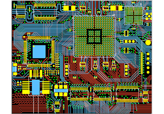
PCB Layout Ability
Maximum signal design speed rate: 10Gbps CML difference signal;
Maximum number of PCB Layout layers: 40 layers;
Minimum line: 2.4mil;
Minimum line distance: 2.4mil;
Minimum BGA PIN distance: 0.4mm;
Minimum machine hole diameter: 6mil;
Minimum beam diameter: 4mil;
Maximum PIN number :; 63000+
Maximum number of original cases: 3600;
Most BGA numbers: 48+