What Is Solder Mask Opening?
Generally, the leads on the PCB are covered with solder mask to prevent short circuits and equipment damage. The so-called solder mask opening is to remove the solder mask layer on the wire so that the wire can be exposed to tin.
What’s The Purpose of Solder Mask Opening in PCB Design?
Solder Mask Opening in PCB design can not only realize the PCB as a plug-and-play plug-in, but also increase the thickness of the solder to achieve the purpose of allowing high current.
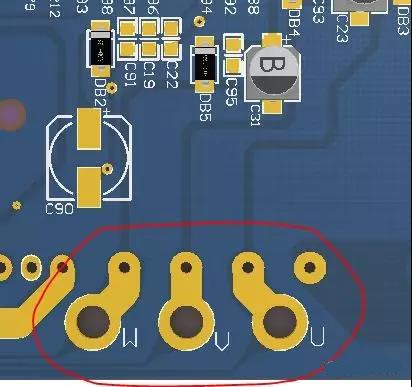
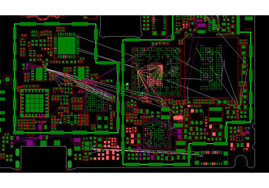
As shown in the figure above, solder mask opening. It is common for PCBs to design as solder mask opening, and the most typical one may be a memory stick. Anyone who takes apart the computer knows that there is a gold finger on the memory stick, as shown in the figure below:
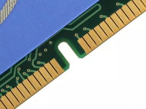
In this case, gold finger is design as solder mask opening, plug and play.
Apart from that, solder mask opening also has a ordinary function, that is, the later iron increases the thickness of the copper foil, which is convenient for heavy current, which is widely used on the power supply board and the motor control board.
How can we design solder mask opening?
In PCB Design, threading and opening can be set on the TOP/BOTTOM SOLDER Layer.
TOP/BOTTOM SOLDER : It is applied to prevent tin on the copper foil and maintain insulation.
Therefore, solder mask opening is able to set on this layer to the pads, vias and non-electrical traces of this layer.
1. In PCB design, the solder pad will be opened by default (OVERRIDE: 0.1016mm), that is, the solder pad exposes the copper foil, expands by 0.1016mm, and solder is applied during the wave soldering process. It is recommended not to make any design changes to ensure solderability;
2. In the PCB design, the vias will be opened by default (OVERRIDE: 0.1016mm), that is, the via has exposed copper foil, expanded by 0.1016mm, and has wave soldering tin. If the design is to prevent SOLDER from pasting on SOLDER MASK, you must select the PENTING option of SOLDER MASK to close SOLDER MASK.
3. In addition, non-electrical wiring can also be carried out separately in this layer, so that the solder mask can be blocked and be opened accordingly. If it is on a copper foil wire, it is used to enhance the ability of the wire to heavy current. Tin is added during the soldering process. If you use non-copper wire, usually used for logo and special character screen printing, you can omit it to create a character screen layer.