Newbies often confuse “PCB schematic” and “PCB design file” when talking about printed circuit boards, but they actually refer to different things. Understanding the differences between them is the key to successfully manufacturing PCBs.
1. What is PCB?
Before jumping into the difference between schematic and design, what needs to be understood is, what is a PCB?
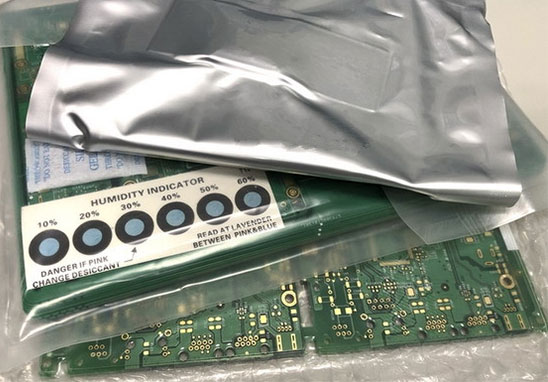
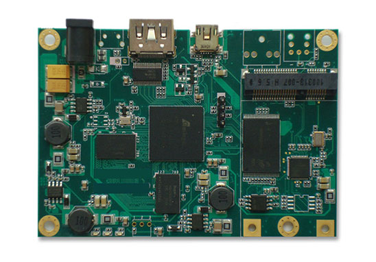
There are basically printed circuit boards inside electronic devices, also known as printed circuit boards. This green circuit board made of precious metal connects all the electrical components of the device and enables it to function properly. Without a PCB, electronics would not work.
2. PCB schematic and PCB design
A PCB schematic is a simple two-dimensional circuit design showing the function and connectivity between different components. The PCB design is a three-dimensional layout, and the position of the components is marked after ensuring the normal operation of the circuit.
Therefore, the PCB schematic is the first part of designing a printed circuit board. It is a graphical representation, whether in written or data form, that uses agreed symbols to describe circuit connections. It also hints at the components that will be used and how they will be connected.
As the name suggests, a PCB schematic is a plan, a blueprint. It does not say where the components will be placed specifically. Rather, the schematic lays out how the PCB will ultimately achieve connectivity and forms a key part of the planning process.
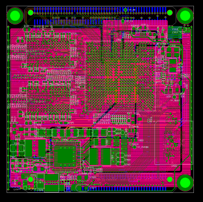
Once the blueprint is complete, the next step is the PCB design. A design is the layout or physical representation of a PCB schematic, including the layout of copper traces and holes. The PCB design shows the location of the above components, and their connections to the copper.
PCB design is a performance-related stage. Engineers build real components on the basis of the PCB design, allowing them to test that the device is working properly. We mentioned earlier that anyone should be able to understand a PCB schematic, but its functionality is not easily understood by looking at a prototype.
Once both of these stages have been completed and you are satisfied with the performance of the PCB, it needs to be implemented by the manufacturer.
3. PCB schematic elements
With a general understanding of the difference between the two, let’s take a closer look at the elements of a PCB schematic. As we mentioned, all connections are visible, but there are a few things to keep in mind:
In order to be able to see the connections clearly, they are not created to scale; on the PCB design they may be very close to each other
Some connections may cross each other, which is practically impossible
Some connections may be on opposite sides of the layout, marked to indicate they are linked
This PCB “blueprint” can take one, two or even a few pages to depict everything that needs to be included in the design
A final note is that more complex schematics can be grouped by function for better readability. Arranging the connections in this way does not happen in the next stage and the schematics often do not match the final design of the 3D model.
4. PCB Design Elements
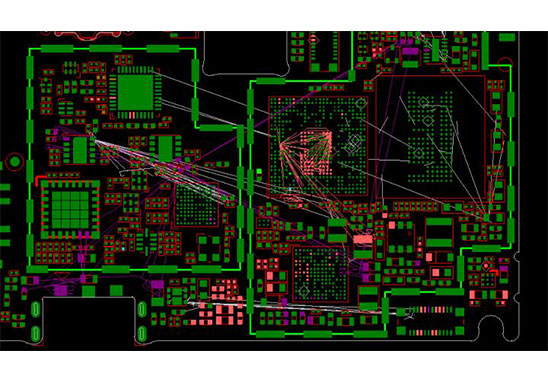
Now is the time to dig deeper into the elements of a PCB design file. At this stage, we transition from written blueprints to physical representations constructed using laminate or ceramic materials. Some more complex applications require the use of flexible PCBs when a particularly compact space is required.
The content of the PCB design file follows the blueprints developed by the schematic flow, however, as mentioned before, the two are very different in appearance. We’ve discussed PCB schematics, but what differences can be observed in design files?
When we talk about a PCB design file, we are talking about a 3D model that includes the printed circuit board and design files. They can be single or multiple layers, although two layers are the most common. We can observe some differences between PCB schematic and PCB design files:
All components are correctly sized and positioned
If two points should not be connected, you must detour or switch to another PCB layer to avoid crossing each other on the same layer
Also, as we touched briefly, PCB design is more concerned with actual performance as this is to some extent the validation phase of the final product. At this point, the practicality that the design must actually work comes into play, and the physical requirements of the printed circuit board must be considered. Some of these include:
How the spacing of components allows adequate heat distribution
Connectors on the edge
How thick the various traces must be regarding current and thermal issues
Design files include silkscreen layers as physical limitations and requirements mean that PCB design files often look very different from the design on the schematic. This silkscreen layer indicates letters, numbers and symbols to help engineers assemble and use the board.
Requires that all components work as planned after they are assembled on the printed circuit board. If it can’t, it needs to be repainted.
Conclusion
Although PCB schematics and PCB design files are often confused, actually making a PCB schematic and PCB design refer to two separate processes when creating a printed circuit board. A PCB schematic that draws the process flow must be created before the PCB design can be performed, which is an important part of determining the performance and integrity of the PCB.