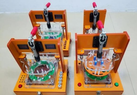
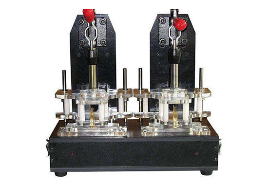
A PCBA Test Jig is a custom test equipment for testing Assembled PCB. When making PCBA Test Jig, PCBA Factory usually need provide Gerber files and PCBA samples to facilitate the production of test jigs.
Steps of Making PCBA Test Jig
1. Material preparation
After the plan is determined according to the pcba data, it is necessary to prepare hardware materials (electronic components), related additional peripheral circuits, equipment, frame materials (such as acrylic boards), glue, electric batch, screws, wire materials, etc., to determine the data for the PCBA Test Jig Making plan.
2.The Determination & Inspection of The Test Jig structure
3. Wiring Requirements
1)The opening of the wire needs to be opened within 2mm. First tin the opening of the wire and the tin position of the test pin.
2)The welded wire should not have swing and loosening phenomenon.
3) Separate the strong and weak wires in the test jig and tie the wires with wires.
4.)The joints of the ammeter and the voltmeter must be installed with a multimeter pen. Banana plugs cannot be installed to test current, voltage and other functions to ensure the safety of the operator.
5)The signal line of the connection of the high-frequency product model must use a shielded wire to ensure the safety of the grounding of the external network.
6) If there is a fire bull in the measuring frame, the casing of the fire bull must be grounded.
7)The fuse must be installed on the test jig, and it cannot be replaced by wires or other wires. Remove the 13A fuse on the original plug. When replacing the fuse, pay attention to how much current the model under test needs. The replacement principle is determined by the working current of the product. 8 -10 times is enough.
4. Quality Inspection of selected Points
Point selection must follow the principles of comprehensive, effective and economical.
The Purpose of PCBA Test Jig
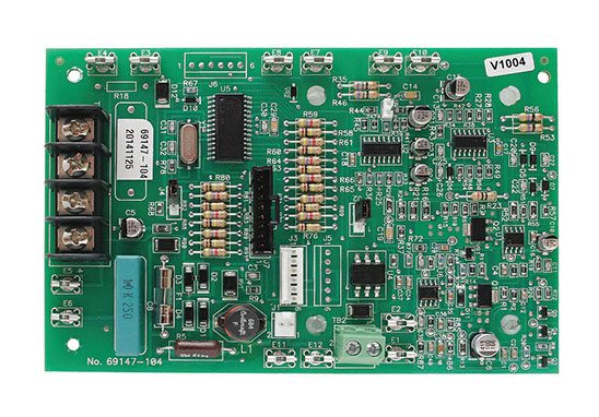
The PCBA Test Jig is widely used in the entire PCB Assembly and Production process. It is mainly used to test the PCBA board after the SMT Assembly and Through-Hole Soldering are completed. Among them, the ICT (In Circuit Test) is mainly used, that is, the electrical conductivity of the circuit board is tested through the test point performance, so as to determine whether the entire PCB board is soldered successfully. The PCBA test jig is the main tool used to assist in completing this test.
The quality of the PCBA Test Jig is related to the efficiency and pass-through rate of the ICT. Due to its long-term and frequent operation, it has high requirements for its production quality, so PCBA manufacturers need pay highly attention to.