The popularity of high-speed serial buses has made more and more differential signals on the PCB. Then, how to perform differential lines in PCB design?
PCB Design Differential Lines Routing Requirements
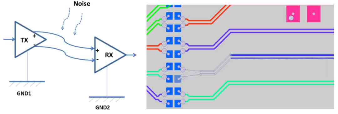
The impedance requirements of various differential lines are different. According to the PCB design requirements, the differential impedance and the corresponding line width spacing are calculated by the impedance calculation software, and set to the constraint manager. Differential lines are coupled to each other to reduce common-mode interference, and should be routed in parallel as far as possible, and there should be no vias or other signals between the two lines. To reduce the loss, ground vias can be added near the layer-changing holes when the high-speed differential line is changed.
Differential Lines Routing Operation Skills In PCB Design
1. Activate the routing command, select the Route→connect command, and then select the defined differential signal line. At this time, the defined differential line will be pulled out at the same time.
2. Support single-line routing mode. When single-line routing mode is required for local routing, click the right mouse button in the routing command state, and select from the pop-up shortcut menu.
Single Trace Mode command mode.
3. When differential lines routing is placed in a small space, you can switch to Neck Mode. Also, click the right mouse button in the routing command state, and select the Neck Mode command in the pop-up shortcut menu.
4. Select the appropriate differential via pattern in the light of the routing requirements. Click the right mouse button in the routing instruction state, and select the Via Pattern command in the pop-up shortcut menu.
Grande Design Capability
Maximum signal design rate: 10Gbps CML differential signal;
Maximum PCB design layers: 40 layers;
Minimum line width: 2.4mil;
Minimum line spacing: 2.4mil;
Minimum BGA PIN spacing: 0.4mm;
Minimum mechanical hole diameter: 6mil;
Minimum laser drilling diameter: 4mil;
Maximum number of PINs: ;63000+
Maximum number of components: 3600;
Maximum number of BGAs: 48+.
PCB Design Service Process
1. The customer provides schematic to inquiry PCB design;
2. Grande evaluates the quotation according to the schematic and customer PCB design requirements;
3. The customer confirms the quotation, signs the contract, and prepays the project payment;
4. Afrer receiving advance payment, Grande starts to arrange Layout Engineer to layout;
5. Once the layout completed, Grande provides a screenshot of the document to the customer for confirmation;
6. The customer confirms OK, settles the balance, and provides PCB design information.