In the PCBA factory, the production of the circuit board will perform a panel operation, so why does PCBA factory assemble PCB as panel way? What are the benefits of PCBA panel?
Why Does PCBA Factory Assemble PCB As Panel Way?
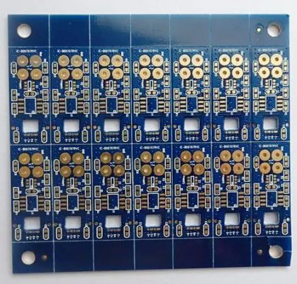
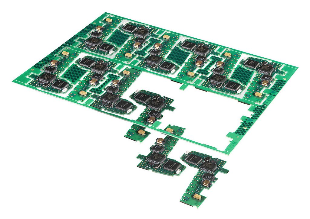
In the process of PCB Assembly and production, a puzzle operation will be carried out in the production of circuit boards in general PCBA factories. Whether it is a PCBA factory or PCB design stage, they will add the edge of the board. The purpose of this process is to increase the production efficiency of SMT Assembly processing. Because the track of the placement machine has a maximum and minimum size limit; For instance, the maximum size of the board can pass through 570mm*750mm, and the minimum size can pass through the 350mm*400mm size, which requires the boards can’t be too big or too small.
This can be found if you often go to the production workshop of the PCBA SMT Assembly factory. Moreover, during SMT Assembly, the most labor-hour consumption is currently the link of solder paste printing. First of all, let’s not talk about the time of solder paste printing and programming, that is, the process of brushing solder paste, regardless of the size of the assembled PCB, in order to ensure that the solder paste can be evenly coated on the PCBA pad paper, the time required for printing must be guaranteed as 20s around, because in contrast, when the placement machine is for component placement, several components can be printed in one second.
What Are The Benefits of PCBA Panel Production?
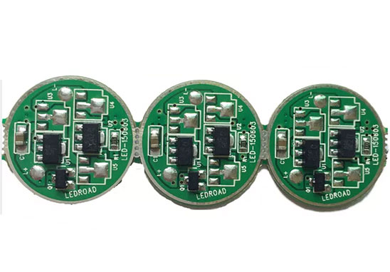
If PCB assembles not as panel way, even if the size of a single board can pass the track of the placement machine. Choosing every singl piece board to grind slowly is not only a waste of the production capacity of the placement machine, but also irresponsible for the production efficiency. So if we put the boards together like 10pcs, 20pcs to assemble, in this way, the mounting pass-through rate of PCB Assembly light board printing solder paste and SMT Assembly in a short time can be improved. There are fewer wires to change, and the circuit board has less time to circulate on the track, which naturally improves the efficiency. In this way, the utility of a single device is maximized as well as the profit margin of the company is improved.
To some degreee, PCBA panel production is also another cost-saving way for the customers, because once the printed circuit board is completed assembly, a great number of testing are required, such as burn-in test, programming test, ICT test, signal test, etc., Then in The circulation time in the production workshop is relatively long, and the storage space after SMT Assembly is also a huge requirement. If it is stored in panels, then no need too much trays; Aslo panel PCBA can be tested evenly, which can save the board. Man-hours wasted when picking and placing in fixtures.
Grande PCBA Capability
1. Maximum Board: 310mm*410mm(SMT);
2. Maximum Board Thickness: 3mm;
3. Minimum Board Thickness: 0.5mm;
4. Minimum Mounted Components: 0201 package or components above 0.6mm*0.3mm;
5. Maximum Weight of Mounted Components: 150 grams;
6. Maximum Component Height: 25mm;
7. Maximum Component Size: 150mm*150mm;
8. Minimum Pin Spacing: 0.3mm;
9. Minimum Spherical Component (BGA) Spacing: 0.3mm;
10. Minimum Spherical Component (BGA) Ball Diameter: 0.3mm;
11. Maximum Components Placement Accuracy (100QFP): 25um@IPC;
12. SMD Capacity: 3-4 million points/day.
Advantages Grande Circuit Board Assembly
1)Strength Guarantee
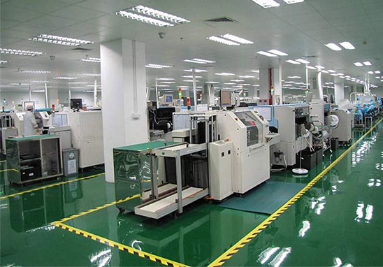
▪ SMT factory: With imported SMT machines and multiple optical inspection equipment, which is able to produce 4 million points per day. Each process is equipped with QC personnel who will keep an eye on product quality.
▪ DIP production line: Two wave soldering machines and more than 10 employees who have worked for over three years. That’ s to say, these workers are highly skilled and can weld various SMT & DIP components.
2)Quality Assurance With High Cost Performance
▪ High-end equipment can paste precision special-shaped parts, BGA, QFN, 0201 package. It can also be soldered prototype pcba via SMT machine and placing bulk materials by hand.
▪ Both samples, small and large batches can be produced. And there is no SMT Machine starting cost.
3)Rich Electronic Products SMT Soldering Experience With Stable Delivery
▪ Accumulated services to thousands of electronics companies, involving SMT soldering services for various types of automotive equipment and industrial control motherboards. Furthermore, PCBA Products are often exported to Europe and the United States, and the quality is able to be affirmed by new and regular customers.
4)Strong Maintenance Ability & Reliable After-Sales Service
▪ The maintenance engineers have sophisticated experience so that those defective boards caused by all kinds of smt soldering can be repaired. Meanwhile, ensuring the connectivity rate of each circuit board also make sense.
▪Order problems feedback will get response, solution and solved as soon as possible.