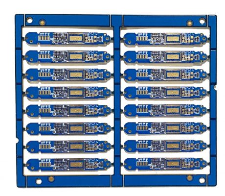
As we all know, the PCBA manufacturing process is a quite complex process. The entire PCBA process seems to be only one word different from PCB. However, as a matter of fact, it varies a lot, that is PCBA has a series of back-end processes based on PCB, such as solder paste printing, SPI (Solder Paste Inspection), SMT Assembly, reflow soldering, DIP soldering, wave soldering/selective wave soldering, PCBA first article inspection, etc. These PCBA process is that the PCB does not come with it.
Just because all subsequent processes are based on the PCB board, the quality of the PCB determines the quality of the entire PCBA. So which aspects of the PCB have an impact on the PCBA?
1. Dirty Board
Dirty board surface is mainly caused by high flux solid content, too large coating amount, too high or too low preheating temperature, too dirty PCB gripper of conveyor belt, too much oxide and tin dross in tin bath, etc.
The main solution is to choose the appropriate flux; control the amount of flux coating; control the preheating temperature; Check the cleaning effect of the automatic cleaning PCB gripper and take measures; clean the oxide and tin slag on the surface of the tin bath in time.

2. White Residue
The white residue on the PCB is often referred to as white frost. Although it does not affect the surface insulation resistance, the customer does not accept it.
Solution: First of all, we can try to use flux and then use solvent to clean; If it cannot be cleaned, it may be due to the aging of the flux, or it may be exposed to the air to absorb water vapor, or it may be due to the high moisture content in the cleaning agent (solvent), or the The flux does not match the cleaning agent, please ask the supplier to help solve or replace the flux cleaning agent.
3. PCB Deformation
PCB deformation is mainly caused by excessive PCB quality or uneven component layout.
When designing the PCB, try to distribute the components as evenly as possible. Design a support strip in the middle of the large-size PCB (the design width of the non-layout component area is 2~3mm); Or use a mass balance tool to press the sparse components on the PCB during the soldering process to achieve mass balance.
Grande PCB Manufacturing Pros
1)Energy production 2 to 14 layers, 14-22 layers can be produced by prototype
2)Minimum line width/spacing: 3mil/3mil BGA spacing: 0.20MM
3)Minimum aperture of finished product: 0.1mm Size: 610mmX1200mm
4)Solder Mask: Japan Tamura, Taiyo, Futoken;
5)FR4: Shengyi, Kingboard, Haigang, Hongren, Guoji, Hazens, South Asia,
(Shengyi S1130/S1141/S1170), Tg130℃/ Tg170℃ Tg180℃ and other high TG plates)
6)High frequency board: Rogers (Rogers), Taconic, ARLLON;
7)Surface technology: spray tin, lead-free spray tin, immersion gold, full board gold plating, plug gold plating, full board thick gold, chemical immersion tin (silver), anti- oxidation (OSP) blue glue, carbon oil.