Schematic Reverse in PCB reverse engineering is a common item. Grande, a professional PCB Reverse Engineering company with more than 10 years of practical experience in the circuit board reverse engineering, which can provide circuit board revision, schematic reverse, chip model identification, chip decryption, PCB reverse engineering and PCB Prototype, and One- Stop PCBA EMS Service.
What is PCB Reverse Engineering?
PCB reverse engineering, on the premise of existing electronic products and circuit boards, reverse R&D technology is used to reversely analyze the circuit boards, and the original products’ PCB files, Bill of Materials (BOM) files, Schematic files and other technical documents and 1:1 reduction of PCB silk screen production files. Then use these technical documents and production documents for PCB Fabrication, component spldering, flying probe test, circuit board debugging, and finish the completed copy of the original sample circuit board.
The use of PCB Reverse Engineering
For PCB reverse engineering, many people do not really understand what is PCB reverse engineering; And some people even think that PCB reverse engineering is a copycat (Shan Zhai in Chinese). In everyone’s understanding, Shan Zhai means imitation, but PCB reverse engineering is definitely not imitation. The purpose of PCB reverse engineering is to learn the latest foreign electronic circuit design technology, and absorb excellent design solutions, then use it to develop and design more excellent product.
With the continuous development and deepening of the PCB reverse engineering industry, today’s PCB reverse engineering concept has been extended to a wider range, no longer limited to simple circuit board copying and cloning, but also involves the secondary development of products and new products.
For instance, by understanding and discussing the analysis of existing product technical documents, design ideas, structural features, process technology, it can provide feasibility analysis and competitive reference for the R&D design of new products, and assist R&D and design units to keep up with the latest updates. Technological development trends, timely adjustment and improvement of product design plans, and research and development of the most competitive new products in the market.
The process of PCB reverse engineering is able to realize the rapid update, upgrade and secondary development of various types of electronic products through the extraction and partial modification of technical data files. Willing to optimize the design and modify the PCB. In addition, it can also add new functions to the product or redesign the functional characteristics on this basis, so that the products with new functions will appear at the fastest speed and with a new attitude, not only have their own intellectual property rights, but also win the first opportunity in the market and bring double benefits to customers.
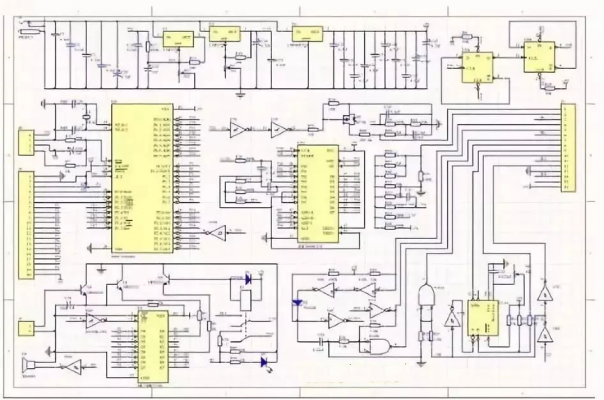
Whether it is used to analyze circuit board principles and product operating characteristics in reverse research, or reused as the basis and basis for PCB design in forward design, PCB schematics have a special role.
Schematic reverse method In PCB reverse engineering
1. Record PCB Related Details
Get a PCB, first record the models, parameters, and positions of all components on the paper, especially the direction of diodes, triodes, and the direction of IC notch. It is best to take two pictures of the component locations with a digital camera. Many PCB circuit boards are getting more and more advanced, and some of the diodes and triodes above are not visible at all.
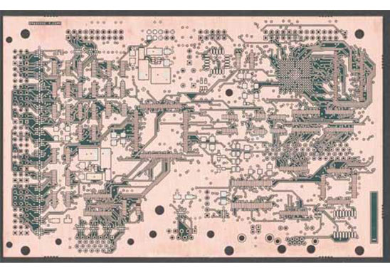
2. Scanned Image
Remove all components and remove the tin from the PAD holes. Clean the PCB with alcohol, and then put it into the scanner. When the scanner scans, you need to slightly increase the scanned pixels to get a clearer image. Then lightly polish the top and bottom layers with water gauze paper until the copper film is shiny, put it into the scanner, start PHOTOSHOP, and scan the two layers in color.
Note that the PCB must be placed horizontally and vertically in the scanner, otherwise the scanned image will not be available.
3. Adjust The Corrected Image
Adjust the contrast and brightness of the canvas to make the part with copper film and the part without copper film have a strong contrast, then turn the secondary image to black and white, check whether the lines are clear, if not, repeat this step. If it is clear, save the picture as TOP BMP and BOT BMP files in black and white BMP format. If there is any problem with the picture, you can also use PHOTOSHOP to repair and correct it.
4. Check The Position Coincidence of PAD & VIA
Convert the two BMP format files to PROTEL format files respectively, and transfer two layers in PROTEL. For example, the positions of PAD and VIA after the two layers are basically the same, indicating that the first few steps are well done. If there is any deviation, then Repeat step three. Therefore, PCB copying is a work that requires great patience, because a little problem will affect the quality and the matching degree after copying.
5. Drawing Layers
Convert the BMP of the TOP layer to the TOP PCB, pay attention to convert it to the SILK layer, which is the yellow layer, and then you can trace the line on the TOP layer, and place the device according to the drawing in the second step. After painting, delete the SILK layer. Repeat until all layers are drawn.
6. Record PCB related details
TOP PCB and BOT PCB combined picture
7. Laser Printing TOP LAYER, BOTTOM LAYER
Use a laser printer to print the TOP LAYER and BOTTOM LAYER on the transparent film (1:1 ratio), put the film on the PCB, and compare whether there is any error. If it is correct, you are done.
8. Test
Test whether the electronic performance of the copy board is the same as that of the original board. If so then it’s really done.
Attention Points During Schematic reverse
1. Reasonable division of functional areas
In the reverse design of the schematic of a complete PCB circuit board, the reasonable division of functional areas can help engineers reduce unnecessary troubles and improve the efficiency of drawing.
Generally speaking, components with the same function on a PCB will be centrally arranged, and the functional division of the area can provide a convenient and accurate basis for inferring the schematic diagram. However, the division of this functional area is not arbitrary, which requires engineers to have a certain understanding of electronic circuit related knowledge.
First, find out the core components in a functional unit, and then in the light of the trace connection, you can find other components of the same functional unit to form a functional partition (the formation of functional partitions is the basis for schematic drawing). In addition, in this process, don’t forget to make clever use of the component serial numbers on the circuit board, they can help you to divide the function faster.
2. Find The Right Reference
This reference part can also be said to be the main component PCB network city used at the beginning of the schematic drawing. After the reference parts are determined, drawing according to the pins of these reference parts can ensure the accuracy of the schematic to a greater extent.
For engineers, the determination of reference parts is not very complicated. Generally speaking, the components that play a major role in the circuit can be selected as reference parts. They are generally larger in size and have more pins, which are convenient for drawing. Such as integrated circuits, transformers, transistors, that can be used as a suitable reference.
3. Correctly Distinguish The Traces & Draw the Trace Reasonably
For the distinction between ground wires, power wires, and signal wires, engineers also need to have relevant power supply knowledge, circuit connection knowledge, PCB wiring knowledge, and so on. The distinction of these circuits can be analyzed from the connection of components, the width of the copper foil of the circuit, and the characteristics of the electronic product itself.
In the trace drawing, in order to avoid trace crossing and interspersed, a large number of grounding symbols can be used for grounding traces, different traces of different colors can be used for various traces to ensure clear and distinguishable traces, and special signs can also be used for various components. The unit circuits are drawn separately and combined at the end.
4. Master The Basic Framework & Learn From Similar Schematic
For the frame composition and schematic drawing method of some basic electronic circuits, engineers need to be proficient, not only to be able to directly draw the basic composition of some simple and classic unit circuits, but also to be able to form the overall frame of the electronic circuit.
On the other hand, don’t ignore that the same type of electronic products have certain similarities in the schematic diagrams. Engineers can make full use of similar circuit diagrams to reverse the new product schematics based on the accumulation of experience.
5. Check & Optimize
After the schematic is drawn, the reverse design of the PCB Schematic can only be said to be completed after a test and verification process. The nominal values of components that are sensitive to PCB distribution parameters need to be checked and optimized. According to the PCB file diagram, the schematic is compared, analyzed and checked to ensure that the schematic and the file diagram are completely consistent.