The simple truth of PCB design is that it must be suitable for its intended application. Therefore, as a PCB design engineer, you will find that there are plenty of different PCB size and shape requirements.
1. Understand the size and shape requirements of the PCB before starting PCB Layout
Apparently, aggressive scheduling and design delay annoyances can be met, and it’s understandable why some PCB layout designers have an eye-opening to start their PCB designs. The problem, of course, is that they may be missing critical design information, especially when it comes to size or form factor or board form factor. Medium design changes are a reality when it comes to PCB layout. One thing you need to do that is to deepen the impact of future changes without complete information from the start. Without good board profile data to work on up front, you’ll have the risk that have to do tremendous redesign later.
To avoid such problems, make sure you understand the size and shape requirements of your design before you start layout. This includes not only the X and Y dimensions of the board, but also the height constraints. Meanwhile, this will also require working closely with your entire design team to obtain the required information. And don’t hesitate to ask as many questions as possible. You don’t want to suffer later on having to replace a lot of circuits in your design because you didn’t realize there would be mounting holes where you put the main processor.
Once you have the required board data, you can now use several different options to create the board outline.
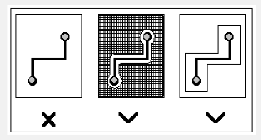
In the past, PCB design tools were more of a hindrance than a help when drafting objects such as circuit board outlines. Fortunately, these tools have evolved over the years, and users now have several options for creating circuit board outlines.
You can draw a layout tool utility that allows designers to manually draw their board outlines. These tools will not only create the main outline for you, but will also add additional outlines for placement and routing constraints. Additionally, you can use the drawing functions in the tool to manipulate outlines and create arcs or other graphic features to finalize the desired size and shape.
Many design tools will also provide you with creation wizards that will automate the drafting of the board outline. The wizard not only includes tools to create the board outline, but will also build the board layer stackup and set the basic trace width and spacing size. Such a wizard can save you a lot of time and effort in creating circuit board outlines.
In addition to these drawing tools, modern PCB design CAD systems often provide you with other useful utilities for working with circuit board outlines. A very important feature when dealing with complex board shapes that is the ability to import mechanical CAD data into the PCB database. This data can be in a number of different formats, including DXF, IDF, IDX, and IPC-2581.
Your PCB design CAD system will read these formats and create the board outline accordingly. You can even save these outlines as templates to reuse in new designs. The key, of course, is to use a CAD system that supports all of these different functions.
2.The importance of a complete design tool system
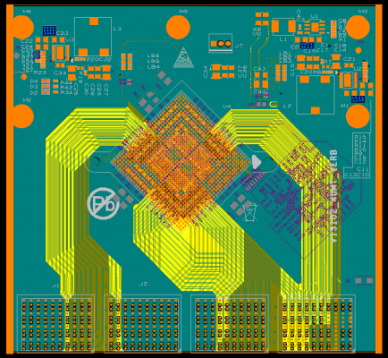
A good PCB design CAD system will not only be able to support different import formats and provide you with plenty of drawing tools, but it will also provide many other benefits. One of the most useful features that is the ability to display both the PCB layout and the mechanical design in the layout tool. This enables designers to see how their layout works throughout the system design. With the 3D capabilities of the layout tool, designers can interactively handle their component placement in real-time and correct any gap errors in the design’s mechanical features.
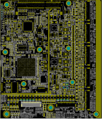
Grande’s PCB Design Capability
Maximum signal design rate: 10Gbps CML differential signal;
Maximum PCB design layers: 40 layers;
Minimum trace width: 2.4mil;
Minimum trace spacing: 2.4mil;
Minimum BGA PIN spacing: 0.4mm;
Minimum mechanical hole diameter: 6mil;
Minimum laser drilling diameter: 4mil;
Maximum number of PINs: ;63000+
Maximum number of components: 3600;
Maximum number of BGAs: 48+.
PCB Design Service Flow
1. The customer provides schematic to inquiry PCB design;
2. Grande evaluates the quotation according to the schematic and customer design requirements;
3. The customer confirms the quotation, signs the contract, and prepays the project deposit;
4. Grande receives advance payment and arranges engineer to design;
5. After the design is completed, Grande provides a screenshot of the document to the customer for confirmation;
6. The customer confirms OK, settles the balance, and Grande provides final PCB design information.