The rapid development of science and technology determines that all enterprises must improve accordingly. Among them, PCBs depend on technology and naturally must not fall behind. Therefore, the layout of high-frequency PCBs has become a key point that everyone need to discuss when designing high-frequency PCBs. Then what are the attention points in high-frequency PCB Design?
Attention Points In High Frequency PCB Design
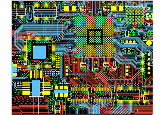
(1) High-frequency circuits tend to have high integration and high-density PCB design routing. Therefore, the use of multi-layer boards is both necessary for PCB design routing as well as an effective means of reducing interference.
(2) The less the lead bends between the pins of the high-speed circuit device, the better. The lead wire of the high-frequency circuit PCB design and routing is preferably a solid line, which need to be wound, and can be folded with a 45° folded line or an arc. To meet this requirement, external transmission and mutual coupling of high-frequency signals can be reduced.
(3) The shorter the lead between the pins of the high-frequency circuit device, the better.
(4) The alternating between the trace layers between the pins of the high-frequency circuit device should be as small as possible. The so-called “minimize interlayer crossover” means that the fewer vias used in the component connection process, the better. It is estimated that one via can bring about 0.5 pF of distributed capacitance. Reduced the number of vias is able to greatly increase the speed.
(5) High-frequency circuit PCB design and layout should pay attention to the “cross-interference” introduced by the parallel traces of the signal traces. If parallel distribution cannot be avoided, a large area “ground” can be placed on the back of the parallel signal traces to greatly reduce interference. Parallel traces in the same layer are almost inevitable, but in two adjacent layers, the traces must be oriented perpendicular to each other.
(6) Grounding measures surrounding particularly important signal traces or local units, that is, drawing the outer contour of the selected object. Using this feature, so-called “packet” processing can be performed automatically on selected important signal traces. Of course, for high-speed systems, it is also very beneficial to use this capability for local processing of components such as clocks.
(7) Various types of signal traces cannot form loops, and ground wires cannot form current loops.
(8) A high frequency decoupling capacitor should be placed near each IC block.
(9) A high frequency turbulent link should be used when connecting the analog ground trace and the digital ground trace to the common ground trace. In the actual assembly of high frequency turbulent chains, high frequency ferrite beads passing through the central hole are often used and are often not represented in circuit schematics and the resulting netlist does not include such components, the PCB design routing will Ignore its existence. Responding to this reality, it can be used as an inductor in the schematic, and the component footprint is individually defined in the PCB Component Library and manually moved to a suitable location near the convergence point of the common ground traces before routing the PCB design.
(10) Analog circuits and digital circuits should be arranged separately. After the independent PCB design is routed, the power and ground traces should be connected at one point to avoid mutual interference.
(11) Before connecting the DSP off-chip program memory and data memory to the power supply, filter capacitors should be added and placed as close as possible to the chip power pins to filter out power supply noise. Also, shielding around the DSP and off-chip program memory and data memory is recommended to reduce external interference.
(12) The off-chip program memory and data memory should be placed as close to the DSP chip as possible. At the same time, the layout should be reasonable so that the lengths of the data lines and address lines are basically the same, especially when there are multiple memories in the system, the clock traces of each memory should be considered. The clock inputs are equally spaced, or a separate programmable clock driver chip can be added.
For the DSP system, the external memory with the same access speed as the DSP should be selected, otherwise the high-speed processing capability of the DSP will not be fully utilized. The DSP instruction cycle is nanoseconds, so the most common problem in DSP hardware systems is high frequency interference. Therefore, when making the printed circuit board (PCB) of the DSP hardware system, special attention should be paid to the address lines and data lines. The routing of the signal trace should be correct and reasonable. When routing, try to keep high-frequency traces short and thick, and keep away from signal traces that are prone to interference, such as analog signal traces. When the circuits around the DSP are more complex, it is recommended to combine the DSP and its clock circuit, reset circuit, off-chip program memory and data memory into a minimal system to reduce interference.
The above is an introduction to the key points of high-frequency PCB design and layout. Grande is a PCB design company specializing in electronic product circuit board layout, which mainly undertakes multi-layer, high-density PCB layout & board prototype business. The PCB layout team with an average of more than 10 years of work experience can proficiently use the mainstream PCB design software in the market, professional and efficient communication to ensure the progress of the PCB design, and help you seize the market opportunities earlier!