1. Common Design Reference of Keying Circuit
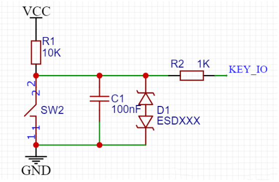
1)The R1 pull-up resistor clamps the uncertain signal at a high level through a resistor, maintaining it in an untriggered state or returning to the original state after being triggered. (Advice to add)
2)The C1 capacitor reduces key jitter and high-frequency signal interference. (Advice to add)
3)R2 current limiting resistor (values ranging from 100 ohms to 10k, if there is an internal pull-up, the value should not be too large, otherwise the current is not enough to pull down the IO port) to protect the IO port to prevent overcurrent and high voltage from burning out the IO It has the effect of absorbing static electricity or some high-voltage pulses. (Advice to add)
4)D1ESD diode Electrostatic protection diode to prevent electrostatic interference or damage to the IO port. (This is based on the cost and protection level requirements of the PCB to decide whether to add or not)
2. Design Reference For External Signal Input (Similar To Keying Circuit)
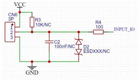
1)The R3 pull-up resistor clamps the uncertain signal to a high level through a resistor, and maintains it in a non-triggered state or returns to the original state after being triggered. (If the external connection line is relatively long and the internal pull-up capability of the chip is relatively weak, it is recommended to add it. Usually the communication distance is not long, and it can be omitted if there is an internal pull-up)
2)C2 capacitor prevents high frequency signal interference. (Note that if the input frequency signal is relatively large, the capacitance value of C2 should be correspondingly reduced, or C2 should be omitted directly)
3)The R4 current limiting resistor protects the IO port to prevent the IO port from being burned out by overcurrent and high voltage, and has the effect of absorbing static electricity or some high-voltage pulses. ( Advice to add )
4)D2ESD diode electrostatic protection diode to prevent electrostatic interference or damage to the IO port. (This is based on the cost and protection level requirements of the PCB to decide whether to add or not)
3. Output Circuit Relay Design Reference
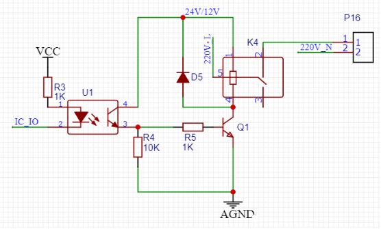
1)U1 optocoupler separates high and low voltage to prevent high voltage interference and achieve electrical isolation.
2)The D5 1N4148 freewheeling diode bai protects the element from being broken down or burned out by the induced voltage. It is connected in parallel to both ends of the element that generates the induced electromotive force, and forms a loop with it, so that the high electromotive force generated by it will continue in the loop. The current consumption is used to protect the components in the circuit from being damaged.
4. Darlington Transistor Design Reference Application
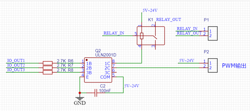
Darlington transistors are generally used in stepper motor drives. In fact, they can be used for motor speed regulation, high-power switching circuits, driving relays, driving LED light sources with relatively high power, and using PWM to adjust the brightness.
1)The R6, R7, and R8 resistors are used to limit the current to prevent the damage of the ULN2001, resulting in the high voltage being directly input to the IO of the MCU (because the ULN2001D itself has a 2.7K resistor, the R6, R7, and R8 can be omitted here. If some driver chips do not have resistors, the most It’s better to add it yourself, you can check the data sheet of the selected chip for the specific situation)
2)COM terminal is connected to the power supply When the output terminal is connected to an inductive load, the load does not need to add a freewheeling diode. The chip is designed with a diode, and only the COM port needs to be connected to the load power supply. When connecting to other loads, the COM port can be left unconnected.
3)When using the RC step-down circuit to supply power to ULN2001D, since the RC step-down voltage cannot prevent the transient high voltage fluctuations on the power grid, a 104 capacitor must be connected to the COM terminal and the ground terminal of the ULN2001D. In other applications, This capacitor may not be added.
5. Operational Amplifier Design Reference Application
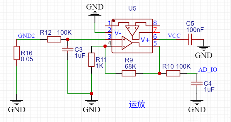
Using the op amp to collect the current current of the load ingeniously, you can accurately know the current operation of the load and whether it is working normally, which is very easy to use. There are also many very delicate and practical circuits in operational amplifiers, which will be shared with you one by one in the future. You can also search online for some classic circuits of operational amplifiers, there are many places for reference.
1)GND2 is the ground terminal of the load. It is connected to the common ground through the R16 resistor (R16 should be selected according to the size of the load current), and there will be a small voltage difference.
2)This circuit is a proportional operation circuit in the same phase, so the voltage of the sampling terminal = the voltage of the input terminal * (1+R9/R11) = 69 times the input voltage. You can modify R9 to adjust the magnification according to the measurement range.
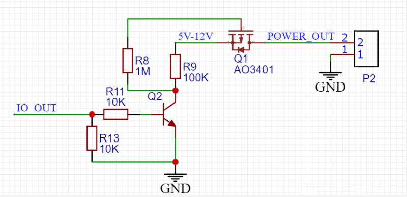
6. MOSFET Design Reference Application (Control Power Output On & Off)
7. Input Power Design Reference Application
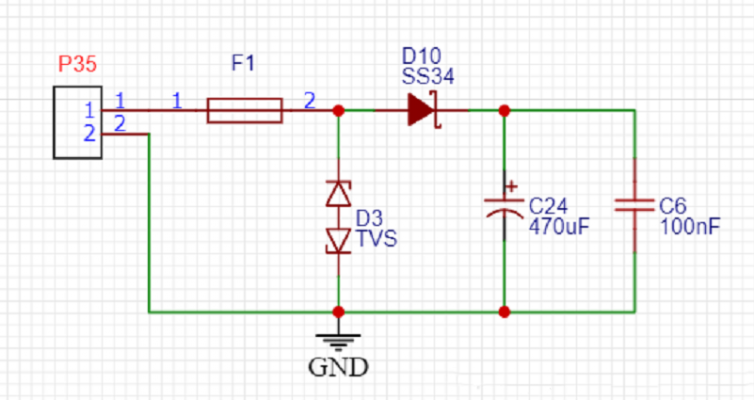
If the circuit cost is relatively tight, components can be appropriately deleted as needed.
1)F1 self-recovery fuse, overcurrent protection, the threshold value can be adjusted according to the actual load current.
2)The D10 Schottky diode reduces the influence of the power supply of the rear stage on the front stage, prevents the positive and negative connections of the power supply from burning out the rear stage circuit, and prevents the current from flowing backward when the power supply is turned off, but there is a voltage drop of about 0.4V through the diode, which needs to be considered. After the 0.4V step-down, will it be lower than the normal working voltage of the subsequent circuit?
3)TVS tube input voltage is too high protection, generally take 1.4 times the normal input voltage.