Tag Archives: pcb layout
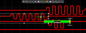
Differential Lines Routing Requirements & Operation Skills In PCB Design
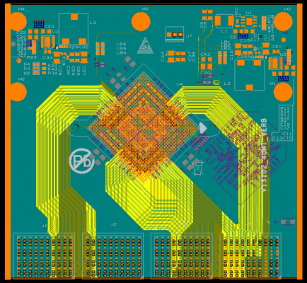
The popularity of high-speed serial buses has made more and more differential signals on the [...]
Apr
Attention Points In High Frequency PCB Design
The rapid development of science and technology determines that all enterprises must improve accordingly. Among [...]
Mar
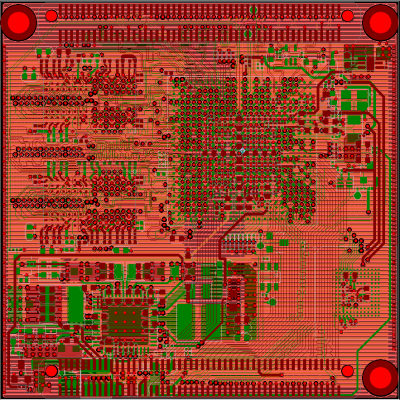
Precautions For Copper Clad In PCB Design
Copper clad is an important part in PCB design. Whether it is domestic PCB design [...]
Mar
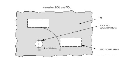
What Are The Requirements & Specifications of Fiducial Mark In PCB Design?
In order to facilitate the assembly of the printed circuit board (PCBA), fiducial mark will [...]
Mar
What Are The Size & Shape Requirements For PCB Design?
The simple truth of PCB design is that it must be suitable for its intended [...]
Feb
What is The General Tolerance In Multilayer PCB Design?
How to Solve The Tolerance Problem in Multilayer PCB Design? No doubt, multilayer PCB is [...]
Dec
When Does PCB Design Safety Require Specific Spacing Rules?
As you probably know, not every PCB Design has the same strict rules like the [...]
Dec
Design Standards of PCB Pads Shape & Size
Design standards of PCB Pads Shape & Size PCB Design is based on the circuit [...]
Nov
PCB Design Standards of Pads Shape & Size
PCB Design is based on the circuit schematic diagram to realize the functions required by [...]
Oct
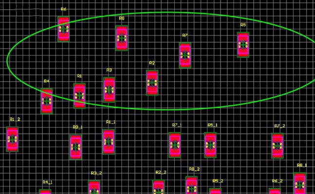
Components Arrangement Discipline In PCB Design
In current PCB design, there are 5 regular disciplines, components arrangement discipline, according to the [...]
Oct