Tag Archives: pcb layout
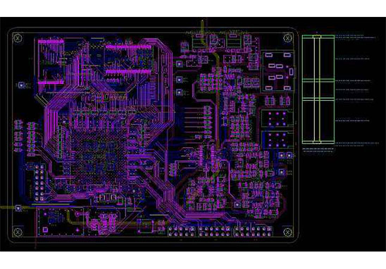
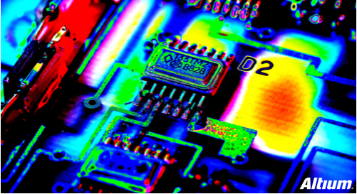
Main Points In PCB Layout
In integrated circuit application design, after the project schematic design is completed, PCB design is [...]
Sep
Why do Pads lost and Pads deformation occur in PADS ( PCB Design Software) ?
At present, most high-speed PCBs are designed via Cadence, PADS software and Altium Designer (AD). However, Companies [...]
Jul
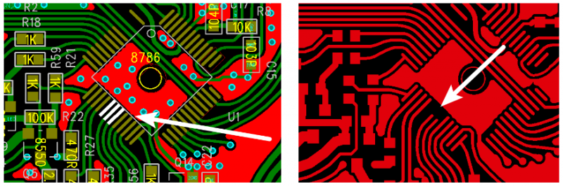
Types of Pads In PCB Layout
What Is Pad? Pad, the basic unit of surface mount assembly, which is used to [...]
Jul
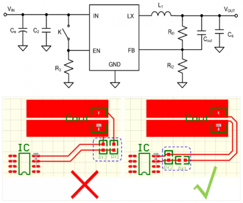
The Role Of Matching Resistors In PCB Design
1.PCB design impedance matching PCB design impedance matching refers to a suitable matching method between [...]
Jul
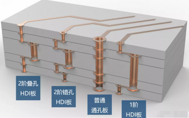
Demystifying The Design Technics of High-End PCB
Plenty of people probably do not know the difference between high-end PCB and common PCB? Because there is not [...]
Jul
Why Most of PCB Layers Are Designed As Even Layer?
I don’t know if you have found such a phenomenon, that is, most of PCB layers are designed as even layers, such [...]
Jul
Why Need Add Fiducial Point & Technological Edge In PCB Design?
Reasons / Adding Fiducial Point When it comes to SMT Assembly, there are usually 3 common methods (based [...]
Jul
Q & A of PCB Layout Knowledge
Q1. What problems should pay attention to when layout high-frequency signals? A1. Impedance matching of the signal [...]
Jul
How Can We Make Good Thermal Management In PCB Layout?
As electronic products continue to be miniaturized as well as more functions are incorporated into smaller devices, [...]
Jul
The Importance Of PCB Laminate Technology For PCB Layout
A good PCB laminate design is essential to reduce the radiation of PCB loops and related circuits. On the [...]
Jul