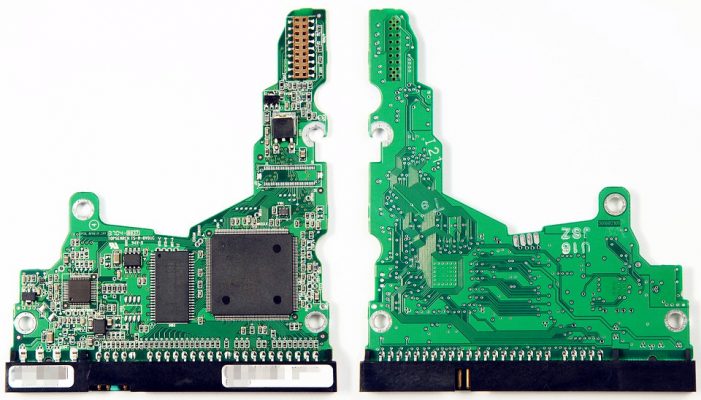
As electronic products continue to be miniaturized as well as more functions are incorporated into smaller devices, the heat dissipation requirements of these systems also increase. This is especially true for PCBs operating at high currents. Especially heavy-duty power supply systems, such as lithium-ion batteries used in electric vehicles, require a power management system integrated on the PCB. Plus high-current drive circuits, heat dissipation need to be emphasized. PCB layout engineer need to implement creative strategies to manage the heat generated in high-current PCBs.
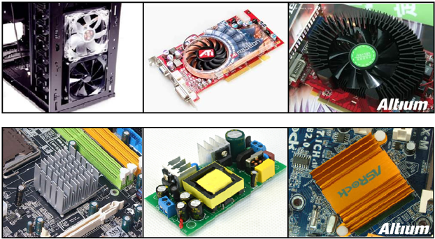
The heat generated by the power loss in the circuit carrying large current should be combed away from the heating device to counter the temperature rise. Everyone may be familiar with fan and radiator used in computer processors. These measures can transfer heat from the circuit board and exchange heat with the circulating air. However, in some PCB components, especially small-size components, fan or radiato may not be installed. This requires consideration of other heat dissipation methods.
1)AdoptThicker Copper For Large Current
The resistance of copper trace and vias is able to cause significant power loss and heat generation in PCB-based components, especially when they carry large currents. Electrical connections with a larger cross-sectional area have lower resistance, which reduces the amount of heat loss.
The amount of copper used in most PCBs is equivalent to about 1 oz per square foot. When it is inconvenient to use a fan or radiator, you can increase the copper thickness. A high-current PCB should use at least twice the amount of copper. Circuits with operating currents exceeding 10 amps should be as high as 3 or 4 oz per square foot.
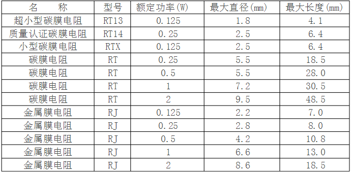
The copper thickness of PCB board is calculated in oz. 1oz means that the average weight of copper foil on a square foot area is 28.35g. oz is the abbreviation of the unit ounce, which is transliterated as “ounce”, which is an imperial unit of measurement and uses the weight per unit area to express the average thickness of the copper foil. Expressed by the formula, 1oz=28.35g/FT2.
Weight Unit: 1oz=28.35g 1 ounce=16 dram 16 ounces=1 pound
Conversion method introduction: The weight of the copper foil divided by the density and surface area of the copper is the thickness of the copper foil.
1 square foot=929.0304 square centimeters, copper density=8.9kg/dm^3
Set Copper thickness as X, and solve the equation:
X*929.0304 square centimeter*8.9 g/cubic centimeter=1oz=28.35g
X=0.0034287 cm=34.287um
So 1oz=34.287um. The thickness of 1oz copper foil is about 35um or 1.35mil.
Using a larger amount of copper requires increasing the trace width on the PCB. In order to avoid occupying too much space area, the trace can also be embedded deeper in the circuit board. For example, placing a copper guide bar. This also helps dissipate heat to the circuit board itself and any nearby heat dissipation holes. Of course, this may require the use of a thicker circuit board, which is suitable for high-current devices.
2) UseHeatDissipation Holes & Thermal Pads
If the air around the heating component does not flow, then which cannot effectively dredge and dissipate heat. The use of heat dissipation holes can transfer heat from key electronic components in the circuit board. Thermal vias are good thermally conductive components between the top and bottom layers of the circuit board. Heat can be transferred to the heat dissipation vias through simple conduction, and then the heat dissipation vias can evacuate the heat from the key electronic components.
The radiator is generally a metal plate installed on the bottom of the circuit board. After the heat dissipation hole transfers heat from the hottest spot of the circuit board itself, it must be transferred to other locations to further dissipate heat from the hottest spot of the circuit board. Generally, the heat dissipation hole transfers heat to the heat dissipation pad for large area heat dissipation.
3)High-PowerComponents Layout
High-current electronic components like microcontrollers generate a lot of heat. It is a good idea to install these components near the center of the circuit board.
If the component is installed near the edge of the circuit board, the heat generated by it will accumulate and the local temperature will be very high. However, if the component is mounted on the middle part of the circuit board, the heat will spread to the entire circuit board, and the temperature of the circuit board will decrease.
Multiple high-power components should be distributed on the entire circuit board, rather than concentrated in one location. If the size of the component allows it, it is even possible to arrange different components separately on different PCB boards. There are several trade-offs in the component layout, because it is related to the realization of the entire circuit board on the one hand, heat dissipation and mechanical matching on the one hand, and the impact that may have on your manufacturing budget.
On the one hand, consider the heat dissipation and mechanical matching, and also consider the impact that may have on your manufacturing budget.
4)AdoptThicker Board
When components operate at extreme temperatures, their electrical connections, components and the life of the circuit board itself will be shortened accordingly. The computer hardware industry has used cooling fans to reduce the risk of this problem. But when the fan does not work, most of the heat directly enters the circuit board and surrounding components. At this time, if the circuit board is very thin, everything will heat up to a very high temperature.
Thicker circuit boards will require more heat when the overall temperature is increased. This thicker circuit board helps keep the temperature on the top of the circuit board low. If the circuit board is directly mounted on the housing, heat can be conducted to the outside of the device. However, this solution may make the production and processing costs higher. Therefore, it needs to be properly weighed when applying.
Let me show you the different board thicknesses used in some of the hardware we made before.
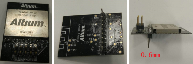
The picture above shows the Wifi module used in the Internet of Things project with a thickness of 0.6mm.
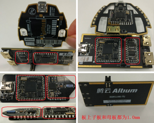
The picture above is a JTAG-USB adapter used for FPGA hardware development, as well as other signal conversion modules, non-high current and high heating circuits. Use 1.0mm plate thickness. The daughter board on the board is used as a small module of similar devices, with a half-hole open, and the edge is gold-plated, and the whole board is soldered to the motherboard as a module. Both the daughter board and the mother board are 1.0mm thick.
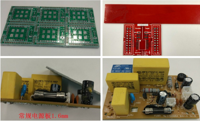
The picture above is a 1.6mm thickness of a conventional power supply board. This 1.6mm is the default thickness of the general board factory. If there is no special instruction, the default is 1.6mm. And the processing cost 1.6mm is the critical point. There is no additional special thickness surcharge within 1.6mm.
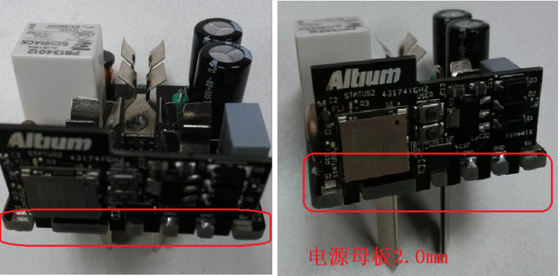
The picture above shows a power socket with a Wifi module that can intelligently remotely control the switch. The motherboard power board adopts 2.0mm thickness. 2.0mm is a thicker plate manufacturing process. The thickness of the board takes into account the high current and high heat generation in a small space.
The best cooling strategy to be adopted depends on many factors. Not all PCB layout or form factors can be adapted to all the above strategies. For example, thermal pads are not suitable for double-sided printed circuit boards. If there are a large number of components on the circuit board, some of them will inevitably be placed near the edge of the circuit board.
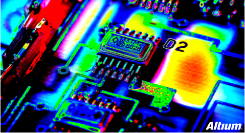
The Altium Designer software tool provides corresponding advanced functions in thermal management, allowing you to visualize potential hot spots in the PCB. Powerful PDN analysis tools enable PCB designers to identify faulty locations that may cause high-current device failures.