Tag Archives: pcb layout
What Is The General Tolerance For Multi-Layer PCB Layout?
Multi layer PCBs are beneficial to products because they can handle greater complexity. Computers, telephones, and [...]
19
Jul
Jul
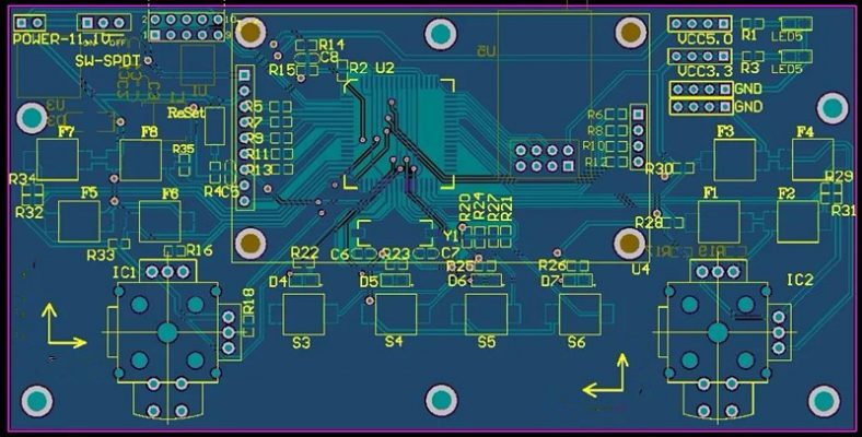
PCB Design & Layout Skills
The following items need to be considered when conveying the Schematic to PCB layout. All the examples mentioned [...]
16
Jul
Jul
The Role Of Matching Resistors In PCB Design
1)PCB design impedance matching PCB design impedance matching refers to a suitable matching method between [...]
09
Jul
Jul
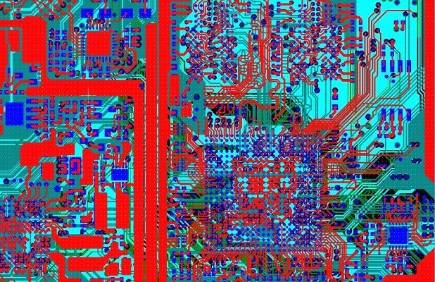
Demystifying The Design Technics of High-End PCB
Plenty of people probably do not know the difference between high-end PCB and common PCB? Because there is not [...]
07
Jul
Jul
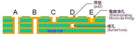
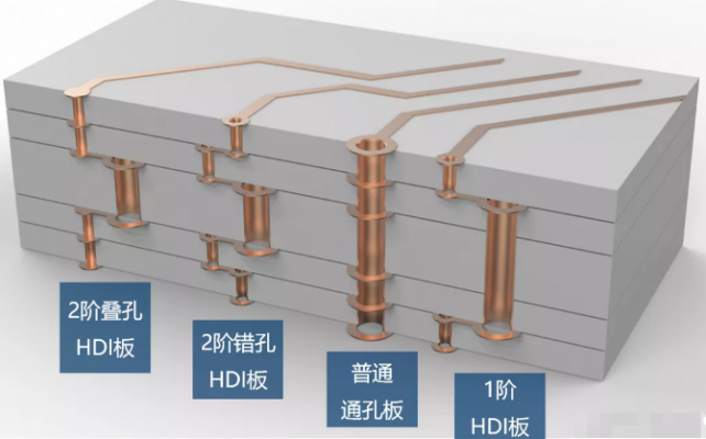
Via-In-Pad Processing Principle
Vias-in-pad or vias-on-pad is a very headache for printed circuit board assembly factories, especially when the vias are placed on [...]
05
Jul
Jul