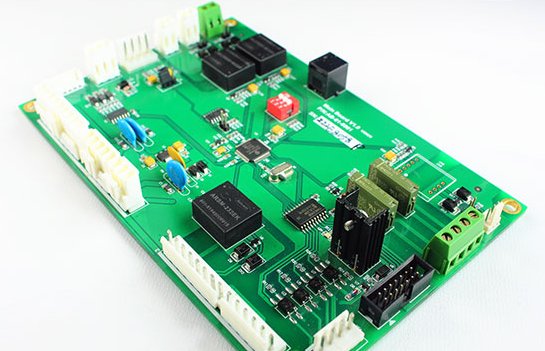
PCB DIP plug-in processing is a very important process in the PCBA chip processing, its processing quality directly affects the functional properties of the PCBA board, so it is necessary to pay more attention to the DIP plug-in process.
DIP plug-in pre-preparation work is more, the basic process is the first plug-in electronic components for processing, the staff according to the BOM to receive materials, check the material type, specifications are correct, according to the PCBA sample board for pre-production processing, the step is to use a variety of related equipment (automatic capacitor shearing machine, jumper bending machine, diode automatic molding machine, automatic band forming machine and other molding equipment) for processing. The basic process is to first process the plug-in electronic components, staff receive the materials according to the BOM bill of materials, check the material type, whether the specifications are correct, pre-processing before production according to the PCBA sample board, the step is to use a variety of related equipment (automatic capacitor foot cutting machine, jumper bending machine, diode automatic forming machine, automatic belt forming machine and other molding equipment) for processing.

Circuit board DIP plug-in processing requires attention to the following points.
1, In the plug-in before, need to check whether the surface of electronic components with oil, paint and other unclean objects.
2, In the plug-in process, must protect the electronic components and PCB flat paste, after the plug-in is completed to protect the electronic components is flush state, do not be uneven, while protecting the plug-in after welding pins can not block the pad.
3, If the electronic components on the direction indicator table, you need to follow the correct direction of the plug-in, do not random plug-in.
4, In the plug-in, you need to pay attention to the force of the plug-in, do not insert too much force, resulting in component damage or PCB board damage.
5, When inserting electronic components do not insert the edge of the PCB board, pay special attention to the height of the electronic components and the spacing between the electronic components.