In the PCB prototype, a layer of lead-tin anticorrosion layer is pre-plated on the copper foil part, which is retained in the outer layer of the board, i.e. the graphic part of the circuit, and then the rest of the copper foil is chemically etched, called etching.
As the last process of PCB from the light board to display the circuit graphics, etching to pay attention to what quality issues? Next, Shenzhen PCB prototype manufacturers – GRANDE PCBA will introduce the PCB prototype etching process considerations.
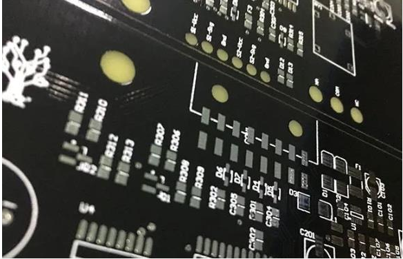
The quality of etching requires complete removal of all copper layers except those under the anticorrosive layer. Strictly speaking, etch quality must include the consistency of line width and the degree of side etching.
The issue of side etching is often discussed in etching. The ratio of side etch width to etch depth is called the etch factor; in the printed circuit industry, a small side etch or low etch factor is most satisfactory. The construction of the etching equipment and the different composition of the etchant can affect the etch factor or degree of side etching.
In many ways, the quality of etching exists long before the board enters the etching machine. Because the various processes of PCB prototyping are very closely and intrinsically linked, there is no process that is not influenced by other processes and does not affect other processes. Many of the problems identified as etch quality are actually already present in the previous film removal process, if not more.
Theoretically, the PCB is proofed into the etching stage. In the pattern plating method, the ideal state should be: the total thickness of copper and lead tin after plating should not exceed the thickness of the plating-resistant photosensitive film, so that the plating pattern is completely blocked by the “wall” on both sides of the film and embedded in it. However, in actual production, the plating pattern is much thicker than the photosensitive pattern; as the coating height exceeds the photosensitive film, there is a tendency of lateral accumulation. The tin or lead-tin corrosion-resistant layer covering the top of the line extends to both sides to form an “edge”, covering a small portion of the photographic film below the “edge”. The “edge” formed by tin or lead-tin makes it impossible to completely remove the photographic film when removing the film, leaving a small part of “residue” below the “edge”, resulting in incomplete etching. Line etching in both sides of the formation of “copper root”, so that the line spacing becomes narrow, resulting in printed boards can not meet customer requirements, and may even be rejected. Scrap will greatly increase the cost of PCB production.
In the PCB prototype, once the etching process problems, it is bound to be batch problems, which will eventually cause great quality risks to the product. Therefore, it is especially important to find the right PCB proofing manufacturer.
GRANDE is a professional printed circuit board manufacturer specializing in printed circuit board manufacturing, 20 years focus on single, double-sided, multilayer circuit board production and production. We can provide impedance board, HDI board, blind buried hole board and other multilayer PCB board prototype, small batch production business.
Our advantages: PCB monthly production capacity of 27,000 square meters | Can do 1-40 layers of high precision circuit board | Domestic four major automotive companies circuit board first-class suppliers | Military cooperation units.