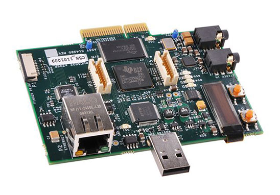
As we all know, there are various reasons for the failure of the PCB circuit board. Only by accurately finding the problem point can the failure be quickly solved.
PCB Circuit Board Fault Detection Method
1. Locate The Fault Position
Once signs of a problem appear, the next step is to track and locate the fault until the fault is identified. Different ways to locate the fault include visual inspection, as well as physical inspection using test equipment. Sure, test techniques rely on high-end test equipment or use basic tools such as multimeters, thermal cameras, magnifiers, and oscilloscopes.
2. Testing Equipment
Typical equipment includes automated flight detection instruments, as well as automated optical inspection (AOI) machines. AOI uses high-resolution cameras to inspect for a variety of defects, including shorts, opens, missing, incorrect or misaligned components.
3. Visual & Physical Inspection
Visual inspection identifies defects such as overlapping traces, shorted solder joints, signs of board overheating, and burned components. When some problems are difficult to identify with the naked eye, a magnifying glass can help identify some short circuits, solder bridges, open circuits, cracks in solder joints and circuit board traces, component offsets, etc.
4. Special Testing Components
When a low resistance is detected between component pins, it is best to remove the component from the PCB circuit and perform a dedicated test. If the resistance is still low, then this component is defective, if not, otherwise further investigation is required.
5. Power Up The Circuit Board For Testing
Visual inspection is only suitable for visual inspection of circuit boards, not for internal layer inspections of circuit boards. If there are no visible defects on the outside, you’ll need to power up the board and perform more detailed testing to see if the board is healthy.
6. Low Voltage Measurement
The technique involves controlling the amount of current passing through the short circuit and finding out where the current is going. Since the copper traces on the circuit board also have resistance, the voltages developed through different parts of the copper traces are also different. With a voltmeter, as you measure the voltage between the different parts along the shorted line, the smaller the voltage, the closer you are to the short.
7. Use Finger To Sense The Heating Area of The Circuit Board
Since short circuits can cause localized temperature rises on the board, finding areas with heat can help find where short circuits are problematic. However, be careful when using power supplies that short copper traces and avoid burns or electric shocks.
8. Repair Short/Open Traces
After identifying the short or open point on the PCB, the next step is to isolate the problem. While this is easy to do on the outer surface of the board, it is a challenge for the inner layers. Possible solutions include drilling through holes or cutting appropriate external copper traces.
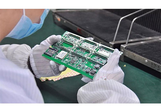
Grande PCBA Advantages
1. Highly Professional: Grande focuses on processing PCB Samples, Small & Medium batches, and promises to deliver within 3-5 working days after the materials are confirmed to be correct.
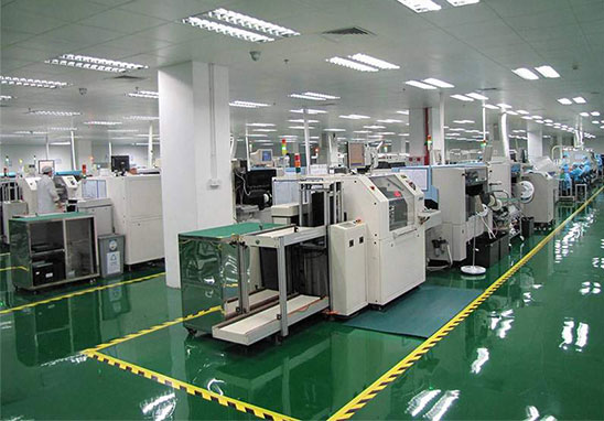
2. Professional Equipment: Grande’s equipment is advanced equipment tailored for sample and small and medium batch production, and can be pasted with 0201, BGA spacing 0.3MM, QFN, CSP, CON and other components.
3. Professional Technology: 100% of technical backbones have more than 5 years of work experience, and 85% of front-line operators have more than 3 years of work experience.
4. Grande implements the 5S and 6σ concepts in daily operations, and it is expected that the shipment will be checked at least 7 times.Grande promises to pass AOI optical inspection if the quantity reaches 100PCS.
5. Grande promises that the soldering pass rate is above 99%. If the customer finds soldering defects, Grande promises to repair it free of charge.