Generally, after PCBA soldering, there will usually be some solder slag left by the solder on the printed circuit board. However, the solder slag must be cleaned up so that it will not affect the use of the circuit board. With the development of science and technology and the improvement of technical personnel, there are many ways to clean up solder slag.
Circuit Board Solder Cleaning Method
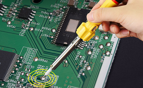
There are two methods for cleaning the solder on the circuit board. One is to clean the solder on the PCBA Board, and the other is to remove the excess solder slag after finishing the soldering work. It is recommended to use a solder sucker to operate. Details please see below:
Firstly, to clean the solder on the PCBA Board
1. Shake off the solder on the soldering iron and melt the solder joints again. Repeat a few times.
2. Find a short section of multi-stranded wire, eat the rosin, melt it together with the solder joints, and remove the wire while it is hot, so that the excess solder can be removed.
3. If there is a large area of solder, special hot air gun or tin furnace can be used.
Secondly, to clean the excess welding slag after welding
1. Use absolute ethanol (or more than 95% alcohol). If it is too dirty, use a soft brush dipped in alcohol.
2. Then blot dry with non-fat cotton.
3. It is more troublesome to use a solder suction device. The double-sided board is more troublesome. The soldering hole uses a needle made by a hospital, and the soldering iron is heated and inserted and rotated. Or you can take a piece of fancy thread (soft thread) and bring it up.
4. Without a tin suction device, you can shake the printing plate quickly to shake off the tin dross after heating. Pay attention to safety and do not move too much. When the soldering iron is soldered, remove the excess solder from the tip of the soldering iron to shake the tin.
Grande PCBA Capacity
1. The largest board: 310mm*410mm (SMT);
2. Maximum board thickness: 3mm;
3. Minimum board thickness: 0.5mm;
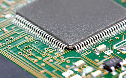
4. The smallest Chip parts: 0201 package or parts above 0.6mm*0.3mm;
5. The maximum weight of mounted parts: 150 grams;
6. Maximum part height: 25mm;
7. Maximum part size: 150mm*150mm;
8. Minimum lead part spacing: 0.3mm;
9. The smallest spherical part (BGA) spacing: 0.3mm;
10. The smallest spherical part (BGA) diameter: 0.3mm;
11. Maximum component placement accuracy (100QFP): 25um@IPC;
12. Mounting capacity: 3 to 4 million points/day.
Why choose Grande?
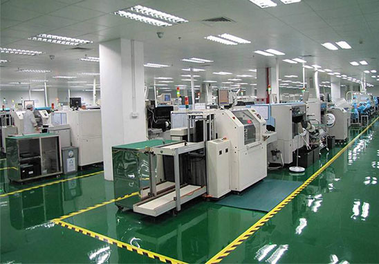
1. Strength Guarantee
▪ SMT workshop: It has imported placement machines and multiple optical inspection equipment, which can produce 4 million points per day. Each process is equipped with QC personnel, who can keep an eye on product quality.
▪ DIP production line: There are two wave soldering machines. Among them, there are more than ten old employees who have worked for more than three years. The workers are highly skilled and can weld all kinds of plug-in materials.
2. Quality Assurance, High Cost Performance
▪ High-end equipment can paste precision shaped parts, BGA, QFN, 0201 materials. It can also be used as a model for mounting and placing bulk materials by hand.
▪ Both samples and large and small batches can be produced.
3. Rich Experience In SMT & Soldering of Electronic Products, Stable Delivery
▪ Accumulated services to thousands of electronic companies, involving SMT chip processing services for various types of automotive equipment and industrial control motherboards. The products are often exported to Europe and the United States, and the quality can be affirmed by new and old customers.
▪ Delivery on time, normal 3-5 days after the materials are complete, and small batches can also be shipped on the same day.
4. Strong Maintenance Ability & Reliable After-Sales Service
▪ The maintenance engineer onws sophisticated experience and can repair the defective products caused by all kinds of patch welding, and ensure the connection rate of each circuit board.
▪ Customer service staff will respond timely and solve your order problems as quickly as possible.