Grande, specialized in providing All-In-One PCBA electronic manufacturing services (EMS), including upstream electronic components procurement to PCB production and Assembly, SMT patch, DIP plug-in, PCBA testing, finished product assembly and other one-stop services. Now, let’s focus on and talk about the anti-static measures in PCB Assembly.
The harm of static electricity to PCBA products
During PCB Assembly, the assembly personnel will insert or mount components in strict accordance with the bill of materials, PCB silk screen and external processing requirements. Even so, the electronic components often generate more or less static electricity without paying attention. These static electricity will release electromagnetic pulses during discharge, which will cause errors in computer operations. In severe cases, it will also cause damage to devices and lines. Only by taking anti-static measures can machines and components be protected.
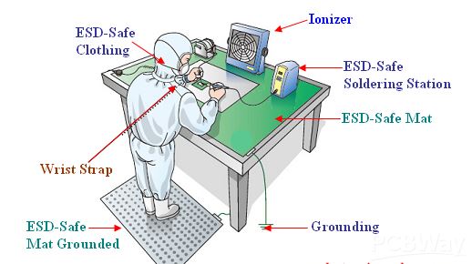
Anti-static measures In PCB Assembly
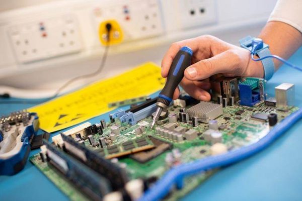
1. All personnel in contact with components and products should wear anti-static clothing, anti-static wristbands, and anti-static shoes.
2. The anti-static system must have a reliable grounding device. The anti-static ground wire shall not be connected to the neutral wire of the power supply and shall not be shared with the lightning protection ground wire.
3. All components are treated as electrostatic sensitive devices.
4. During the operation, use an anti-static work surface, and use an anti-static container for components and semi-finished products.
5. The soldering equipment is reliably grounded, and the electric soldering iron adopts anti-static type, which must be tested before using.
6. Warehouse management personnel should wear anti-static gloves when sending materials and IQC testing, use the instrument to ground reliably, and lay anti-static rubber pads on the work surface.
7. Regularly test the above anti-static tools, settings and materials to confirm that they are in the required conditions.

Grande’s PCBA Capability
1. Maximum board: 310mm*410mm(SMT);
2. Maximum plate thickness: 3mm;
3. Minimum plate thickness: 0.5mm;
4. Minimum chip component: 0201 package or parts above 0.6mm*0.3mm;
5. Maximum weight of mounted component: 150 grams;
6. Maximum component height: 25mm;
7. Maximum component size: 150mm*150mm;
8. Minimum pin spacing: 0.3mm;
9. Minimum spherical component (BGA) spacing: 0.3mm;
10. Minimum spherical component (BGA) ball diameter: 0.3mm;
11. Maximum component placement accuracy (100QFP): 25um@IPC;
12. SMD capacity: 3-4 million points/day.