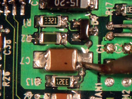
PCBA has requirements for the size of tin beads on the circuit board. This requirement is determined by the customer. In the light of the various products and different customer requirements, the acceptable requirements for tin beads will also be different. Generally, the final Tin Beads Acceptance Standard is based on the national standard and combine with the customer’s requirements.
Tin Bead Acceptance Standard In PCBA Soldering
Some industry standards interpret tin beading. The classification ranges from no tin beads in the MIL-STD-2000 standard to less than 5 per square inch in the IPC-A-610C standard.
In the IPC-A-610C standard, a minimum insulation gap of 0.13 mm is specified, and tin beads with a diameter within this are considered qualified; And tin beads with a diameter greater than or equal to 0.13 mm are unqualified, and the manufacturer must take corrective actions measures to prevent this from happening. The latest version of the IPCA-610D standard for lead-free soldering does not explicitly address solder balling. The requirement for less than 5 solder beads per square inch has been removed. But standards for automotive and military products do not allow any solder balls, so the PCB must be cleaned after soldering, or the solder balls must be removed by hand.
The above is the introduction of the acceptable standards for PCBA Soldering tin beads.
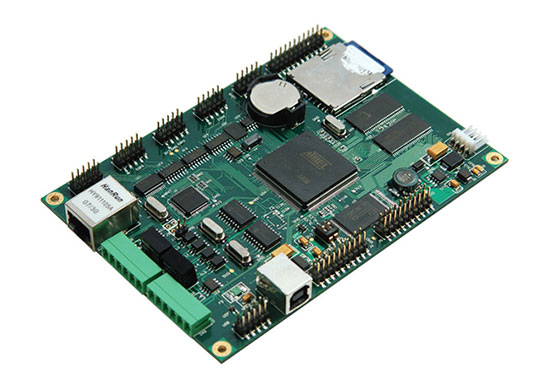
PCBA Capability
1. Maximum Board: 310mm*410mm(SMT);
2. Maximum Board Thickness: 3mm;
3. Minimum Board Thickness: 0.5mm;
4. Minimum SMD Component: 0201 package or components above 0.6mm*0.3mm;
5. Maximum Weight of Mounted Component: 150 grams;
6. Maximum Component Height: 25mm;
7. Maximum Component Size: 150mm*150mm;
8. Minimum Pin Spacing: 0.3mm;
9. Minimum Spherical Component (BGA) Spacing: 0.3mm;
10. Minimum Spherical Component (BGA) Ball Diameter: 0.3mm;
11. Maximum Component Placement Accuracy (100QFP): 25um@IPC;
12. SMD Capacity: 3-4 million points/day.

Advantages of PCB Assembly In Grande
1. Highly Professional: Grande focuses on PCBA samples, small and medium batches; For 2 Layer Simple Sample PCBA, Grande promises to deliver within 3-7 working days after the materials are confirmed to be OK.
2. Professional Equipment: Advanced equipment tailored for sample and small and medium batch production, and can be pasted with 0201, BGA spacing 0.3MM, QFN, CSP, CON and other components.
3. Professional Technology: 100% of technical backbones have more than 5 years of work experience, and 85% of front-line operators have more than 3 years of work experience.
4. Grande implements the 5S and 6σ concepts in daily operations, and it is expected that the shipment will be checked at least 7 times.
5. Grande promises that the soldering pass rate is above 99%. If the customer finds soldering defects, the company promises to repair it free of charge.