The harm of static electricity to PCBA boards
During PCB Assembly, processing personnel will strictly follow the bill of materials, PCB silk screen and outsourcing processing requirements to insert or mount components, but electronic components often generate more or less static electricity without paying attention. These static electricity will emit electromagnetic pulses during discharge, which will cause errors in computer calculations. In severe cases, it will cause damage to devices and circuits. Only by taking electrostatic prevention measures can you protect machines and components.
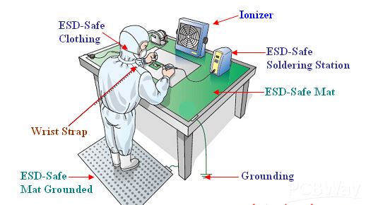
PCBA electrostatic prevention measures
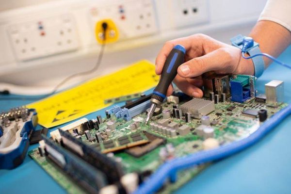
1) All personnel who come into contact with components and products wear anti-static clothes, anti-static bracelets, and anti-static shoes.
2)The anti-static system must have a reliable grounding device.That’s to say, the anti-static ground wire must not be connected to the power neutral wire or shared with the lightning protection ground wire.
3)All components are treated as electrostatic sensitive devices.
4)During the operation, use ananti-staticwork surface, and use anti-static containers for components and semi-finished products.
5)The welding equipment is grounded reliably, and the electric soldering iron is of anti-static type, which must be tested before use.
6)Warehouse management personnel should wear anti-static gloves when sending materials and IQC inspections, use meters to be grounded reliably, and anti-static rubber pads on the work surface.
7)Periodically inspect the above-mentioned anti-static tools, settings and materials to confirm that they are in the required conditions.
PCB Assembly Capability
1)The largest board: 310mm*410mm (SMT);
2)Maximum board thickness: 3mm;
3)Minimum board thickness: 0.5mm;
4)The smallest Chip parts: 0201 package or parts above 0.6mm*0.3mm;
5)The maximum weight of the mounted parts: 150 grams;
6)Maximum part height: 25mm;
7)The largest part size: 150mm*150mm;
8)Minimum lead part spacing: 0.3mm;
9)The smallest spherical part (BGA) spacing: 0.3mm;
10)The smallest spherical part (BGA) diameter: 0.3mm;
11)Maximum component placement accuracy (100QFP): 25um@IPC;
12)Mounting capacity: 3 to 4 million points/day.

Why Choosing Grande To Do Small Batch SMT Assembly?
1)Strength Guarantee
▪ SMT factory: With imported SMT machines and multiple optical inspection equipment, which is able to produce 4 million points per day. Each process is equipped with QC personnel who will keep an eye on product quality.
▪ DIP production line: Two wave soldering machines and more than 10 employees who have worked for over three years. That’ s to say, these workers are highly skilled and can weld various SMT & DIP components.
2)Quality Assurance With High Cost Performance
▪ High-end equipment can paste precision special-shaped parts, BGA, QFN, 0201 package. It can also be soldered prototype pcba via SMT machine and placing bulk materials by hand.
▪ Both samples, small and large batches can be produced. And there is no SMT Machine starting cost.
3)Rich Electronic Products SMT Soldering Experience With Stable Delivery
▪ Accumulated services to thousands of electronics companies, involving SMT soldering services for various types of automotive equipment and industrial control motherboards. Furthermore, PCBA products are often exported to Europe and the United States, and the quality is able to be affirmed by new and regular customers.
4)Strong Maintenance Ability & Reliable After-Sales Service
▪ The maintenance engineers have sophisticated experience so that those defective boards caused by all kinds of smt soldering can be repaired. Meanwhile, ensuring the connectivity rate of each circuit board also make sense.
▪Order problems feedback will get response, solution and solved as soon as possible.