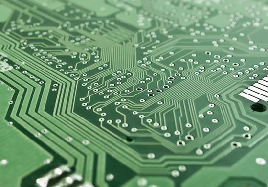
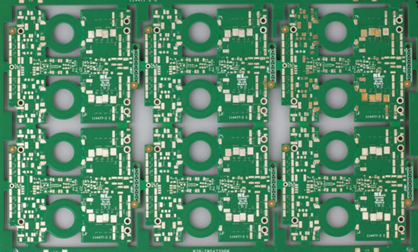
1.PCB size and appearance inspection
PCB size inspection mainly includes the diameter of the processing hole, the spacing and its tolerance, and the small edge of the PCB; While PCB appearance inspection is about the solder mask and the pad alignment, for instance, whether the solder mask has impurities, peeling and wrinkling, the benchmark mark is qualified, the circuit conductor width (line width) and spacing meet the requirements or not.
2.PCB warpage and distortion detection
The basic test principle: the PCB under test is exposed to the thermal environment and carry out the thermal stress test. In addition, a typical thermal stress test method that is a spin dip test and a solder float test. In this test method, a PCB is immersed in molten solder for a certain period of time, and then removed for warpage and distortion detection.
3.Solderability test of PCB
The solderability test of PCB focuses on the test of pads and plated through holes, which includes edge dip test, spin dip test and solder bead test. (The specific test method—Reference IPCS-804)
BTW, the edge dip test is used to test the solderability of surface conductors, the spin dip test and the crest test are used to test the solderability of surface conductors and electrical vias, and the solder bead test is only used to test the solderability of electrical vias.
4.PCB solder mask integrity test
PCBs in SMT are generally adopts dry film solder masks and optical imaging solder masks. These two types of solder masks have high fractions and are not fluid. In order to prevent the potential defects of PCB solder mask, the PCB should be subjected to a strict thermal stress test during incoming inspection. This test mostly uses solder float test, whose testing time is 10-15 around, and the solder temperature is 260-288 ° C or so.
5.PCB internal defect test
Generally, micro-slicing technology is used to test the internal defects of PCBs. (The specific test method—IPC-TM-650) After the solder floating thermal stress test, the PCB is micro-sectioned. The main testing items are the thickness of copper and tin-lead alloy coatings, the alignment of the internal conductors of the multilayer board, the inter-layer gaps and copper cracks.